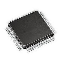
L6460 STMicroelectronics, L6460 Datasheet - Page 109

L6460
Manufacturer Part Number
L6460
Description
MOSFET & Power Driver ICs SPI Config Stepper DC Multi Motor DRV
Manufacturer
STMicroelectronics
Type
Full-Bridge Driverr
Datasheet
1.L6460.pdf
(139 pages)
Specifications of L6460
Product
Half-Bridge Drivers
Rise Time
0.4 us
Fall Time
0.4 us
Supply Voltage (max)
38 V
Supply Voltage (min)
13 V
Supply Current
11 mA
Mounting Style
SMD/SMT
Minimum Operating Temperature
- 40 C
Number Of Drivers
4
Output Current
10 mA
Output Voltage
30 V
Package / Case
TQFP-64
Lead Free Status / RoHS Status
Lead free / RoHS Compliant
Available stocks
Company
Part Number
Manufacturer
Quantity
Price
Company:
Part Number:
L6460
Manufacturer:
MICROCHIP
Quantity:
998
L6460
22.6
GPIO[5]
The GPIO[5] truth table is (for the abbreviation list please refer to
Table 46.
1. Master bit is at logic level “1” when
2. This bit is at logic level “1” if AUX1 regulator is a system regulator but its power stage is externally realized
3. In all configurations in which GPIO[5] is enabled as output:
Master
(and therefore the regulation loop is not used to drive bridge 3). In this case Vloop1IsSys bit will be at logic
level “1”, while Vloop1OnMtr3SideA and Vloop1OnMtr3SideB bits will be at logic level “0” in
CoreConfigReg register.
a) the GPIO[5] pin can be always used as an analog input to the ADC system (ADC function) by writing its
b) the GPIO[5] pin can be always used as a digital input so its value can be always read through SPI
c) the GPIO[5] pin is a rail to rail, back to back output supplied by V
1
0
0
0
0
0
0
0
0
0
0
address in the A2DChannelX[4:0] in the A2DConfigX register and starting a conversion;
interface (SPI_IN function);
(1)
external
GPIO[5] truth table
system
Vloop1
AUX1
and
X
1
0
0
0
0
0
0
0
0
0
(2)
enable[5]
GpioOut
X
X
0
1
1
1
1
1
1
1
1
Doc ID 17713 Rev 1
L6460
GPIO[5] SPI BITS
Mode[2] Mode[1] Mode[0]
X
X
X
0
0
0
0
1
1
1
1
is used as a master device
X
X
X
0
0
1
1
0
0
1
1
X
X
X
0
1
0
1
0
1
0
1
3v3
(seeChapter
.
Comp1OUT inverted
AuxPwm3 inverted
SPI OUT inverted
Table
Reg Loop1 OUT
Reg Loop1 OUT
Reg Loop1 OUT
Slave control
HiZ (SPI_IN)
Comp1OUT
AuxPwm3
Function
SPI OUT
inverted
8)
40).
GPIO pins
109/139
Note
(3)
(3)
(3)
(3)
(3)
(3)
(3)
(3)
(3)


