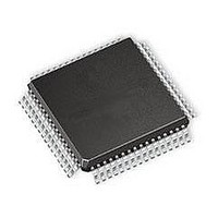
L6460 STMicroelectronics, L6460 Datasheet - Page 129

L6460
Manufacturer Part Number
L6460
Description
MOSFET & Power Driver ICs SPI Config Stepper DC Multi Motor DRV
Manufacturer
STMicroelectronics
Type
Full-Bridge Driverr
Datasheet
1.L6460.pdf
(139 pages)
Specifications of L6460
Product
Half-Bridge Drivers
Rise Time
0.4 us
Fall Time
0.4 us
Supply Voltage (max)
38 V
Supply Voltage (min)
13 V
Supply Current
11 mA
Mounting Style
SMD/SMT
Minimum Operating Temperature
- 40 C
Number Of Drivers
4
Output Current
10 mA
Output Voltage
30 V
Package / Case
TQFP-64
Lead Free Status / RoHS Status
Lead free / RoHS Compliant
Available stocks
Company
Part Number
Manufacturer
Quantity
Price
Company:
Part Number:
L6460
Manufacturer:
MICROCHIP
Quantity:
998
L6460
23
23.1
Serial interface
L6460 can communicate with an external microprocessor by using an integrated slave SPI
(serial protocol interface). Through this interface almost all L6460 functionalities can be
controlled and all the ICs can be seen as a register map made by 128 register of 16-bit
each.
The SPI is a simple industry standard communications interface commonly used in
embedded systems and it has the following four I/O pins:
The “MISO” (master in, slave out) signal carries synchronous data from the slave to the
master device. The MOSI (master out, slave in) signal carries synchronous data from the
master to the slave device. The SCLK signal is driven by the master, synchronizing all data
transfers. Each SPI slave device has one nSS signal that is an active-low slave input/master
output pin. Slave devices do not respond to transactions unless their nSS input signal is
driven low. Master device interfacing with multiple SPI slave devices has an nSS signal for
each slave device.
L6460 will maintain its MISO pin in high impedance until it does not recognize its address in
serial frame.
Read transaction
A read transaction (see
nSS pin. The other bits are then sent on the MOSI pin with this order:
1.
2.
3.
4.
At this point the data stored in the register at the selected address will be shifted out on the
MISO pin.
The read operation is terminated by raising the signal on nSS pin.
–
–
–
–
7-bit representing the address of the register that must be read (MSB first [A
2-bit that must be “10” for a read transaction;
2-bit representing L6460 IC address;
1-bit reserved for future use that must be set at “0”.
MISO (master input slave output)
MOSI (master output slave input)
SCLK (serial clock [controlled by the master])
nSS (slave select active low [controlled by the master])
Figure
Doc ID 17713 Rev 1
45) is always started by the master device that lowers the
Serial interface
6
…A
129/139
0
]);


