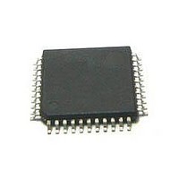
MC56F8245VLD Freescale Semiconductor, MC56F8245VLD Datasheet - Page 37

MC56F8245VLD
Manufacturer Part Number
MC56F8245VLD
Description
DSC 48K FLASH 60MHZ 44-LQFP
Manufacturer
Freescale Semiconductor
Series
56F8xxxr
Datasheets
1.TWR-56F8257.pdf
(88 pages)
2.MC56F8245VLD.pdf
(14 pages)
3.MC56F8245VLD.pdf
(2 pages)
4.MC56F8245VLD.pdf
(629 pages)
Specifications of MC56F8245VLD
Core Processor
56800E
Core Size
16-Bit
Speed
60MHz
Connectivity
CAN, I²C, LIN, SCI, SPI
Peripherals
LVD, POR, PWM, WDT
Number Of I /o
35
Program Memory Size
48KB (24K x 16)
Program Memory Type
FLASH
Ram Size
3K x 16
Voltage - Supply (vcc/vdd)
3 V ~ 3.6 V
Data Converters
A/D 8x12b, D/A 1x12b
Oscillator Type
Internal
Operating Temperature
-40°C ~ 105°C
Package / Case
44-LQFP
Product
DSCs
Processor Series
56800E
Core
56800E
Device Million Instructions Per Second
60 MIPs
Maximum Clock Frequency
60 MHz
Number Of Programmable I/os
35
Data Ram Size
6 KB
Operating Supply Voltage
3.3 V
Maximum Operating Temperature
+ 105 C
Mounting Style
SMD/SMT
Minimum Operating Temperature
- 40 C
On-chip Adc
12 bit, 4 Channel
Package
44LQFP
Family Name
MC56F82xx
Maximum Speed
60 MHz
Data Bus Width
16 Bit
Interface Type
I2C/SCI/SPI
On-chip Dac
1-chx12-bit
Number Of Timers
8
Lead Free Status / RoHS Status
Lead free / RoHS Compliant
Eeprom Size
-
Lead Free Status / Rohs Status
Details
Available stocks
Company
Part Number
Manufacturer
Quantity
Price
Company:
Part Number:
MC56F8245VLD
Manufacturer:
FREESCAL
Quantity:
269
Company:
Part Number:
MC56F8245VLD
Manufacturer:
Freescale Semiconductor
Quantity:
10 000
Each of these sources has an associated bit in the reset status register (RSTAT) in the system integration module (SIM).
The external pin reset function is shared with a GPIO port A7 on the RESET/GPIOA7 pin. The reset function is enabled
following any reset of the device. Bit 7 of the GPIOA_PER register must be cleared to use this pin as a GPIO port pin. When
the pin is enabled as the RESET pin, an internal pullup device is automatically enabled.
5.4
The on-chip clock synthesis (OCCS) module allows designers using an internal relaxation oscillator, an external crystal, or an
external clock to run 56F8000 family devices at user-selectable frequencies up to 60 MHz.
The features of OCCS module include:
The clock generation module provides the programming interface for the PLL, internal relaxation oscillator, and crystal
oscillator. It also provides a postscaler to divide clock frequency down by 1, 2, 4, 8, 16, 32, 64, 128, or 256 before feeding it to
the SIM. The SIM is responsible for further dividing these frequencies by 2, which ensures a 50% duty cycle in the system clock
output. For details, refer to the OCCS section of the device’s reference manual.
5.4.1
When an external frequency source or crystal is not used, an internal relaxation oscillator can supply the reference frequency.
It is optimized for accuracy and programmability while providing several power-saving configurations that accommodate
different operating conditions. The internal relaxation oscillator has little temperature and voltage variability. To optimize
power, the internal relaxation oscillator supports a run state (8 MHz), standby state (400 kHz), and a power-down state.
During a boot or reset sequence, the relaxation oscillator is enabled by default (the PRECS bit in the PLLCR word is set to 0).
Application code can then also switch to the external clock source and power down the internal oscillator, if desired. If a
changeover between internal and external clock sources is required at power-on, ensure that the clock source is not switched
until the desired external clock source is enabled and stable.
To compensate for variances in the device manufacturing process, the accuracy of the relaxation oscillator can be incrementally
adjusted to within + 0.078% of 8 MHz by trimming an internal capacitor. Bits 0–9 of the oscillator control (OSCTL) register
allow you to set an additional offset (trim) to this preset value to increase or decrease capacitance. Each unit added or subtracted
changes the output frequency by about 0.078% of 8 MHz, allowing incremental adjustment until the desired frequency accuracy
is achieved.
The center frequency of the internal oscillator is calibrated at the factory to 8 MHz, and the TRIM value is stored in the flash
information block and loaded to the HFM IFR option register 0 at reset. When using the relaxation oscillator, the boot code
should read the HFM IFR option register 0 and set this value as OSCTL TRIM. For further information, refer to the device’s
reference manual.
5.4.2
The internal crystal oscillator circuit is designed to interface with a parallel-resonant crystal resonator in the frequency range,
specified for the external crystal, of 4 MHz to 16 MHz. A ceramic resonator can be substituted for the 4 MHz to 16 MHz range.
When used to supply a source to the internal PLL, the recommended crystal/resonator is in the 8 MHz to 16 MHz range to
optimize PLL performance. Oscillator circuits appear in
Freescale Semiconductor
•
•
•
•
•
•
•
Software reset (SWR)
Ability to power down the internal relaxation oscillator or crystal oscillator
Ability to put the internal relaxation oscillator into standby mode
Ability to power down the PLL
Provides a 2x system clock that operates at two times the system clock to the timer and SCI modules
Safety shutdown feature if the PLL reference clock is lost
Ability to be driven from an external clock source
On-chip Clock Synthesis
Internal Clock Source
Crystal Oscillator/Ceramic Resonator
MC56F825x/MC56F824x Digital Signal Controller, Rev. 3
Figure 9
and
Figure
10.
Follow the crystal supplier’s recommendations
General System Control Information
37


