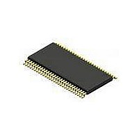
PCF85176T/1,118 NXP Semiconductors, PCF85176T/1,118 Datasheet - Page 38

PCF85176T/1,118
Manufacturer Part Number
PCF85176T/1,118
Description
IC LCD DISPLAY DVR 40SEG 56TSSOP
Manufacturer
NXP Semiconductors
Datasheet
1.PCF85176T1118.pdf
(43 pages)
Specifications of PCF85176T/1,118
Package / Case
56-TFSOP (0.240", 6.10mm Width)
Display Type
LCD
Configuration
40 Segment
Interface
I²C
Current - Supply
20µA
Voltage - Supply
1.8 V ~ 5.5 V
Operating Temperature
-40°C ~ 85°C
Mounting Type
Surface Mount
Number Of Digits
20
Number Of Segments
40
Maximum Clock Frequency
2640 Hz
Operating Supply Voltage
1.8 V to 5.5 V
Maximum Power Dissipation
400 mW
Maximum Operating Temperature
+ 95 C
Attached Touch Screen
No
Maximum Supply Current
20 uA
Minimum Operating Temperature
- 40 C
Lead Free Status / RoHS Status
Lead free / RoHS Compliant
Digits Or Characters
-
Lead Free Status / Rohs Status
Details
Other names
568-5933-2
PCF85176T/1,118
PCF85176T/1,118
Available stocks
Company
Part Number
Manufacturer
Quantity
Price
Part Number:
PCF85176T/1,118
Manufacturer:
NXP/恩智浦
Quantity:
20 000
NXP Semiconductors
PCF85176_1
Product data sheet
15.3 Wave soldering
15.4 Reflow soldering
Key characteristics in wave soldering are:
Key characteristics in reflow soldering are:
Table 20.
Table 21.
Moisture sensitivity precautions, as indicated on the packing, must be respected at all
times.
Studies have shown that small packages reach higher temperatures during reflow
soldering, see
Package thickness (mm)
< 2.5
≥ 2.5
Package thickness (mm)
< 1.6
1.6 to 2.5
> 2.5
•
•
•
•
•
Process issues, such as application of adhesive and flux, clinching of leads, board
transport, the solder wave parameters, and the time during which components are
exposed to the wave
Solder bath specifications, including temperature and impurities
Lead-free versus SnPb soldering; note that a lead-free reflow process usually leads to
higher minimum peak temperatures (see
reducing the process window
Solder paste printing issues including smearing, release, and adjusting the process
window for a mix of large and small components on one board
Reflow temperature profile; this profile includes preheat, reflow (in which the board is
heated to the peak temperature) and cooling down. It is imperative that the peak
temperature is high enough for the solder to make reliable solder joints (a solder paste
characteristic). In addition, the peak temperature must be low enough that the
packages and/or boards are not damaged. The peak temperature of the package
depends on package thickness and volume and is classified in accordance with
Table 20
SnPb eutectic process (from J-STD-020C)
Lead-free process (from J-STD-020C)
and
Figure
All information provided in this document is subject to legal disclaimers.
21
27.
Rev. 01 — 14 April 2010
Package reflow temperature (°C)
Volume (mm
< 350
235
220
Package reflow temperature (°C)
Volume (mm
< 350
260
260
250
3
3
)
)
Universal LCD driver for low multiplex rates
Figure
350 to 2000
260
250
245
27) than a SnPb process, thus
≥ 350
220
220
PCF85176
245
> 2000
260
245
© NXP B.V. 2010. All rights reserved.
38 of 43


