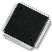
XC68HC12A0CPV8 Freescale Semiconductor, XC68HC12A0CPV8 Datasheet - Page 363

XC68HC12A0CPV8
Manufacturer Part Number
XC68HC12A0CPV8
Description
IC, 16BIT MCU, 68HC12, 8MHZ, TQFP-112
Manufacturer
Freescale Semiconductor
Datasheet
1.MC912D60ACFUE8.pdf
(460 pages)
Specifications of XC68HC12A0CPV8
Controller Family/series
68HC12
No. Of I/o's
68
Eeprom Memory Size
1KB
Ram Memory Size
2KB
Cpu Speed
8MHz
No. Of Timers
1
Core Size
16 Bit
Program Memory Size
60KB
Peripherals
ADC
Lead Free Status / RoHS Status
Lead free / RoHS Compliant
- Current page: 363 of 460
- Download datasheet (5Mb)
ATD0CTL3/ATD1CTL3 — ATD Control Register 3
MC68HC912D60A — Rev. 3.1
Freescale Semiconductor
RESET:
Bit 7
0
0
6
0
0
READ: any time
WRITE: any time
S1C — Conversion Sequence Length (Least Significant Bit)
FIFO — Result Register FIFO Mode
This control bit works with control bit S8C in ATDCTL5 in determining
how many conversion are performed per sequence.
When the S1C bit is set, a sequence length of 1 is defined. However,
if the S8C bit is also set, the S8C bit takes precedence. For sequence
length coding information see the description for S8C bit in ATDCTL5.
In normal operation, the A/D conversion results map into the result
registers based on the conversion sequence; the result of the first
conversion appears in the first result register, the second result in the
second result register, and so on. In FIFO mode the result register
counter is not reset at the beginning or ending of a conversion
sequence; conversion results are placed in consecutive result
registers between sequences. The result register counter wraps
around when it reaches the end of the result register file. The
conversion counter value in ATDSTAT0 can be used to determine
where in the result register file, the next conversion result will be
placed.
The results register counter is initialized to zero on three events: on
reset, the beginning of a normal (non-FIFO) conversion sequence,
and the end of a normal (non-FIFO) conversion sequence. Therefore,
the reset bit in register ATDTEST1 can be toggled to zero the result
register counter; any sequence allowed to complete normally will zero
the result register counter; a new sequence (non-FIFO) initiated with
a write to ATDCTL4/5 followed by a write to ATDCTL3 to set the FIFO
bit will start a FIFO sequence with the result register initialized.
0 = Result registers maps to the conversion sequence
1 = Result registers do not map to the conversion sequence
5
0
0
Analog-to-Digital Converter
4
0
0
S1C
3
0
FIFO
2
0
FRZ1
1
0
Analog-to-Digital Converter
FRZ0
Bit 0
0
Technical Data
ATD Registers
$0063/$01E3
363
Related parts for XC68HC12A0CPV8
Image
Part Number
Description
Manufacturer
Datasheet
Request
R
Part Number:
Description:
Manufacturer:
Freescale Semiconductor, Inc
Datasheet:
Part Number:
Description:
Manufacturer:
Freescale Semiconductor, Inc
Datasheet:
Part Number:
Description:
Manufacturer:
Freescale Semiconductor, Inc
Datasheet:
Part Number:
Description:
Manufacturer:
Freescale Semiconductor, Inc
Datasheet:
Part Number:
Description:
Manufacturer:
Freescale Semiconductor, Inc
Datasheet:
Part Number:
Description:
Manufacturer:
Freescale Semiconductor, Inc
Datasheet:
Part Number:
Description:
Manufacturer:
Freescale Semiconductor, Inc
Datasheet:
Part Number:
Description:
Manufacturer:
Freescale Semiconductor, Inc
Datasheet:
Part Number:
Description:
Manufacturer:
Freescale Semiconductor, Inc
Datasheet:
Part Number:
Description:
Manufacturer:
Freescale Semiconductor, Inc
Datasheet:
Part Number:
Description:
Manufacturer:
Freescale Semiconductor, Inc
Datasheet:
Part Number:
Description:
Manufacturer:
Freescale Semiconductor, Inc
Datasheet:
Part Number:
Description:
Manufacturer:
Freescale Semiconductor, Inc
Datasheet:
Part Number:
Description:
Manufacturer:
Freescale Semiconductor, Inc
Datasheet:
Part Number:
Description:
Manufacturer:
Freescale Semiconductor, Inc
Datasheet:


