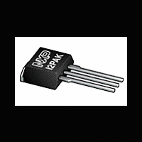
BUK6E3R2-55C NXP Semiconductors, BUK6E3R2-55C Datasheet - Page 7

BUK6E3R2-55C
Manufacturer Part Number
BUK6E3R2-55C
Description
MOSFET,N CH,55V,120A,SOT226
Manufacturer
NXP Semiconductors
Datasheet
1.BUK6E3R2-55C127.pdf
(14 pages)
Specifications of BUK6E3R2-55C
Transistor Polarity
N Channel
Drain Source Voltage Vds
55V
On Resistance Rds(on)
2.7mohm
Rds(on) Test Voltage Vgs
10V
Voltage Vgs Max
16V
Operating Temperature Range
-55°C To +175°C
Transistor Case
RoHS Compliant
Transistor Case Style
I2-PAK
Rohs Compliant
Yes
NXP Semiconductors
Table 6.
BUK6E3R2-55C
Product data sheet
Symbol
Source-drain diode
V
t
Q
rr
Fig 5.
Fig 7.
SD
r
(A)
(S)
g
I
D
250
200
150
100
fs
100
50
75
50
25
0
0
function of gate-source voltage; typical values
drain current; typical values
Transfer characteristics: drain current as a
Forward transconductance as a function of
0
0
Characteristics
Parameter
source-drain voltage
reverse recovery time
recovered charge
20
T
j
= 175 °C
2
40
…continued
60
T
j
= 25 °C
4
V
Conditions
I
see
I
V
80
All information provided in this document is subject to legal disclaimers.
S
S
GS
DS
003aae201
003aae199
= 25 A; V
= 20 A; dI
I
(V)
D
Figure 16
= 25 V
(A)
Rev. 01 — 6 September 2010
100
6
GS
S
/dt = -100 A/µs; V
= 0 V; T
Fig 6.
Fig 8.
j
= 25 °C;
R
(mΩ)
(A)
I
DSon
D
100
N-channel TrenchMOS intermediate level FET
80
60
40
20
10
8
6
4
2
0
0
function of drain-source voltage; typical values
of gate-source voltage; typical values
Output characteristics: drain current as a
Drain-source on-state resistance as a function
GS
0
0
10
= 0 V;
5
0.5
4
5
BUK6E3R2-55C
3.8
Min
-
-
-
10
1
Typ
0.85
67
176
V
1.5
15
GS
© NXP B.V. 2010. All rights reserved.
(V) = 3.6
V
V
003aae290
003aae200
GS
DS
Max
1.2
-
-
(V)
3.4
(V)
3.2
20
2
Unit
V
ns
nC
7 of 14


