PSMN9R0-30LL NXP Semiconductors, PSMN9R0-30LL Datasheet
PSMN9R0-30LL
Specifications of PSMN9R0-30LL


Related parts for PSMN9R0-30LL


PSMN9R0-30LL Summary of contents
Page 1
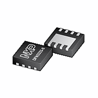
... PSMN9R0-30LL N-channel QFN3333 mΩ logic level MOSFET Rev. 04 — 7 July 2010 1. Product profile 1.1 General description Logic level N-channel MOSFET in QFN3333 package qualified to 150 °C. This product is designed and qualified for use in a wide range of industrial, communications and power supply equipment. ...
Page 2
... avalanche energy unclamped; R Simplified outline Transparent top view SOT873-1 (QFN3333) Description plastic thermal enhanced very thin small outline package; no leads; 8 terminals All information provided in this document is subject to legal disclaimers. Rev. 04 — 7 July 2010 PSMN9R0-30LL Min = Figure 14 Figure 17 °C; - j(init) ≤ ...
Page 3
... Figure °C; see Figure °C mb ≤ 10 µs; T pulsed ° ° j(init) ≤ unclamped sup All information provided in this document is subject to legal disclaimers. Rev. 04 — 7 July 2010 PSMN9R0-30LL Min Max - kΩ -20 20 Figure Figure 226 - 50 -55 150 -55 150 - 260 ...
Page 4
... N-channel QFN3333 mΩ logic level MOSFET 003aae127 P 150 200 ( ° Fig 2. Limit DSon All information provided in this document is subject to legal disclaimers. Rev. 04 — 7 July 2010 PSMN9R0-30LL 120 der (%) 100 Normalized total power dissipation as a function of solder point temperature =10 μ 100 μ 100 ms ...
Page 5
... Transient thermal impedance from junction to mounting base as a function of pulse duration; typical values PSMN9R0-30LL Product data sheet N-channel QFN3333 mΩ logic level MOSFET Conditions see Figure All information provided in this document is subject to legal disclaimers. Rev. 04 — 7 July 2010 PSMN9R0-30LL Min Typ Max - 1.9 4.5 [ 003aae129 t p δ ...
Page 6
... Figure see Figure see Figure 14; see Figure see Figure D DS see Figure MHz °C; see Figure 15 j All information provided in this document is subject to legal disclaimers. Rev. 04 — 7 July 2010 PSMN9R0-30LL Min Typ Max 0 1.3 1.7 2. 2. 100 - 5 100 - 10 11.9 - 14 ...
Page 7
... GS = 4.7 Ω °C G(ext 7 ° see Figure /dt = 100 A/µ 003aae132 (A) D Fig 6. All information provided in this document is subject to legal disclaimers. Rev. 04 — 7 July 2010 PSMN9R0-30LL Min Typ = 0. 150 ° ° Transfer characteristics: drain current as a function of gate-source voltage; typical values ...
Page 8
... V ( 0.75 1 -60 V (V) DS Fig 10. Gate-source threshold voltage as a function of junction temperature All information provided in this document is subject to legal disclaimers. Rev. 04 — 7 July 2010 PSMN9R0-30LL Drain-source on-state resistance as a function max typ min 0 60 120 mA © NXP B.V. 2010. All rights reserved. ...
Page 9
... R DSon (mΩ) typ max Fig 12. Drain-source on-state resistance as a function 03aa27 120 180 ( ° Fig 14. Gate charge waveform definitions All information provided in this document is subject to legal disclaimers. Rev. 04 — 7 July 2010 PSMN9R0-30LL 40 V (V) = 2.6 2 drain current; typical values GS(pl) V ...
Page 10
... C rss (V) DS Fig 16. Source (diode forward) current as a function (V) 8 24V All information provided in this document is subject to legal disclaimers. Rev. 04 — 7 July 2010 PSMN9R0-30LL ( 150 ° 0.3 0.6 source-drain (diode forward) voltage; typical values 003aae137 = 15V (nC) G 003aae138 = 25 ° 0.9 1.2 ...
Page 11
... 2.4 3.4 1.80 0.55 0.52 0.65 1.95 2.2 3.2 1.58 0.45 0.35 REFERENCES JEDEC JEITA - - - - - - All information provided in this document is subject to legal disclaimers. Rev. 04 — 7 July 2010 PSMN9R0-30LL detail 0.1 0.05 0.1 0.1 EUROPEAN PROJECTION SOT873 ISSUE DATE 10-03-10 19-04-10 © NXP B.V. 2010. All rights reserved. ...
Page 12
... NXP Semiconductors 8. Revision history Table 7. Revision history Document ID Release date PSMN9R0-30LL v.4 20100707 • Modifications: Status changed from preliminary to product. PSMN9R0-30LL v.3 20100623 PSMN9R0-30LL Product data sheet N-channel QFN3333 mΩ logic level MOSFET Data sheet status Change notice Product data sheet ...
Page 13
... Export control — This document as well as the item(s) described herein may be subject to export control regulations. Export might require a prior authorization from national authorities. All information provided in this document is subject to legal disclaimers. Rev. 04 — 7 July 2010 PSMN9R0-30LL © NXP B.V. 2010. All rights reserved ...
Page 14
... TrenchMOS, TriMedia and UCODE — are trademarks of NXP B.V. HD Radio and HD Radio logo — are trademarks of iBiquity Digital Corporation. http://www.nxp.com salesaddresses@nxp.com All information provided in this document is subject to legal disclaimers. Rev. 04 — 7 July 2010 PSMN9R0-30LL Trademarks © NXP B.V. 2010. All rights reserved ...
Page 15
... Please be aware that important notices concerning this document and the product(s) described herein, have been included in section ‘Legal information’. © NXP B.V. 2010. For more information, please visit: http://www.nxp.com For sales office addresses, please send an email to: salesaddresses@nxp.com All rights reserved. Date of release: 7 July 2010 Document identifier: PSMN9R0-30LL ...