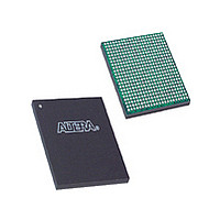
EP3C16F484I7N Altera, EP3C16F484I7N Datasheet - Page 156

EP3C16F484I7N
Manufacturer Part Number
EP3C16F484I7N
Description
Cyclone III
Manufacturer
Altera
Datasheet
1.EP3C16F484I7N.pdf
(274 pages)
Specifications of EP3C16F484I7N
Family Name
Cyclone III
Number Of Logic Blocks/elements
15408
# I/os (max)
346
Frequency (max)
437.5MHz
Process Technology
65nm
Operating Supply Voltage (typ)
1.2V
Logic Cells
15408
Ram Bits
516096
Operating Supply Voltage (min)
1.15V
Operating Supply Voltage (max)
1.25V
Operating Temp Range
-40C to 100C
Operating Temperature Classification
Industrial
Mounting
Surface Mount
Pin Count
484
Package Type
FBGA
Lead Free Status / Rohs Status
Compliant
Available stocks
Company
Part Number
Manufacturer
Quantity
Price
Company:
Part Number:
EP3C16F484I7N
Manufacturer:
ALTERA
Quantity:
4 000
Company:
Part Number:
EP3C16F484I7N
Manufacturer:
ALTERA41
Quantity:
60
Part Number:
EP3C16F484I7N
Manufacturer:
ALTERA/阿尔特拉
Quantity:
20 000
- Current page: 156 of 274
- Download datasheet (6Mb)
8–12
DDR Output Registers
Figure 8–5. Cyclone III Device Family Dedicated Write DDIO
Cyclone III Device Handbook, Volume 1
f
-90° Shifted Clock
A dedicated write DDIO block is implemented in the DDR output and output enable
paths.
Figure 8–5
implemented in the I/O element (IOE) registers.
The two DDR output registers are located in the I/O element (IOE) block. Two serial
data streams routed through datain_l and datain_h, are fed into two registers,
output register Ao and output register Bo, respectively, on the same clock
edge. The output from output register Ao is captured on the falling edge of the
clock, while the output from output register Bo is captured on the rising edge of
the clock. The registered outputs are multiplexed by the common clock to drive the
DDR output pin at twice the data rate.
The DDR output enable path has a similar structure to the DDR output path in the
IOE block. The second output enable register provides the write preamble for the DQS
strobe in DDR external memory interfaces. This active-low output enable register
extends the high-impedance state of the pin by half a clock cycle to provide the
external memory’s DQS write preamble time specification.
For more information about Cyclone III device family IOE registers, refer to the
Cyclone III Device I/O Features
Output Enable
datain_h
datain_l
shows how Cyclone III device family dedicated write DDIO block is
Output Register A
Output Register B
Output Enable
Register A
Output Enable
Register B
Register
Register
Register
Register
chapter.
IOE
IOE
IOE
IOE
DDR Output Enable Registers
DDR Output Registers
Chapter 8: External Memory Interfaces in the Cyclone III Device Family
OE
OE
O
O
data0
data1
data1
data0
®
Cyclone III Device Family Memory Interfaces Features
© January 2010 Altera Corporation
DQ or DQS
Related parts for EP3C16F484I7N
Image
Part Number
Description
Manufacturer
Datasheet
Request
R

Part Number:
Description:
CYCLONE II STARTER KIT EP2C20N
Manufacturer:
Altera
Datasheet:

Part Number:
Description:
CPLD, EP610 Family, ECMOS Process, 300 Gates, 16 Macro Cells, 16 Reg., 16 User I/Os, 5V Supply, 35 Speed Grade, 24DIP
Manufacturer:
Altera Corporation
Datasheet:

Part Number:
Description:
CPLD, EP610 Family, ECMOS Process, 300 Gates, 16 Macro Cells, 16 Reg., 16 User I/Os, 5V Supply, 15 Speed Grade, 24DIP
Manufacturer:
Altera Corporation
Datasheet:

Part Number:
Description:
Manufacturer:
Altera Corporation
Datasheet:

Part Number:
Description:
CPLD, EP610 Family, ECMOS Process, 300 Gates, 16 Macro Cells, 16 Reg., 16 User I/Os, 5V Supply, 30 Speed Grade, 24DIP
Manufacturer:
Altera Corporation
Datasheet:

Part Number:
Description:
High-performance, low-power erasable programmable logic devices with 8 macrocells, 10ns
Manufacturer:
Altera Corporation
Datasheet:

Part Number:
Description:
High-performance, low-power erasable programmable logic devices with 8 macrocells, 7ns
Manufacturer:
Altera Corporation
Datasheet:

Part Number:
Description:
Classic EPLD
Manufacturer:
Altera Corporation
Datasheet:

Part Number:
Description:
High-performance, low-power erasable programmable logic devices with 8 macrocells, 10ns
Manufacturer:
Altera Corporation
Datasheet:

Part Number:
Description:
Manufacturer:
Altera Corporation
Datasheet:

Part Number:
Description:
Manufacturer:
Altera Corporation
Datasheet:

Part Number:
Description:
Manufacturer:
Altera Corporation
Datasheet:

Part Number:
Description:
CPLD, EP610 Family, ECMOS Process, 300 Gates, 16 Macro Cells, 16 Reg., 16 User I/Os, 5V Supply, 25 Speed Grade, 24DIP
Manufacturer:
Altera Corporation
Datasheet:


