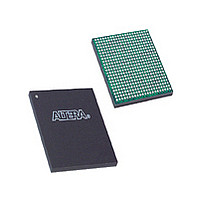
EP3C16F484I7N Altera, EP3C16F484I7N Datasheet - Page 168

EP3C16F484I7N
Manufacturer Part Number
EP3C16F484I7N
Description
Cyclone III
Manufacturer
Altera
Datasheet
1.EP3C16F484I7N.pdf
(274 pages)
Specifications of EP3C16F484I7N
Family Name
Cyclone III
Number Of Logic Blocks/elements
15408
# I/os (max)
346
Frequency (max)
437.5MHz
Process Technology
65nm
Operating Supply Voltage (typ)
1.2V
Logic Cells
15408
Ram Bits
516096
Operating Supply Voltage (min)
1.15V
Operating Supply Voltage (max)
1.25V
Operating Temp Range
-40C to 100C
Operating Temperature Classification
Industrial
Mounting
Surface Mount
Pin Count
484
Package Type
FBGA
Lead Free Status / Rohs Status
Compliant
Available stocks
Company
Part Number
Manufacturer
Quantity
Price
Company:
Part Number:
EP3C16F484I7N
Manufacturer:
ALTERA
Quantity:
4 000
Company:
Part Number:
EP3C16F484I7N
Manufacturer:
ALTERA41
Quantity:
60
Part Number:
EP3C16F484I7N
Manufacturer:
ALTERA/阿尔特拉
Quantity:
20 000
- Current page: 168 of 274
- Download datasheet (6Mb)
9–8
Configuration Process
Cyclone III Device Handbook, Volume 1
f
The output resistance of the repeater buffers must fit the maximum overshoot
equation shown in
Equation 9–1.
Note to
(1)
This section describes the configuration process.
For more information about the configuration cycle state machine of Altera
refer to the
Handbook.
Power Up
If the device is powered up from the power-down state, the V
must be powered up to the appropriate level for the device to exit POR.
To begin configuration, the required voltages listed in
to the appropriate voltage levels.
Table 9–4. Power-Up Voltage for Cyclone III Device Family Configuration
Reset
When nCONFIG or nSTATUS is low, the device is in reset. Upon power-up, the
Cyclone III device family goes through POR. POR delay is dependent on the MSEL
pin settings, which correspond to the configuration scheme that you selected.
Depending on the configuration scheme, either a fast or standard POR time is
available. The fast POR time is 3 ms < TPOR < 9 ms for a fast configuration time. The
standard POR time is 50 ms < TPOR < 200 ms, which has a lower power-ramp rate.
During POR, the device resets, holds nSTATUS and CONF_DONE low, and tri-states all
user I/O pins. When the device exits POR, all user I/O pins continue to tri-state. The
user I/O pins and dual-purpose I/O pins have weak pull-up resistors that are always
enabled (after POR) before and during configuration. After POR, the Cyclone III
device family releases nSTATUS, which is pulled high by an external 10-kΩ pull-up
resistor and enters configuration mode.
When nCONFIG goes high, the device exits reset and releases the open-drain
nSTATUS pin, which is then pulled high by an external 10-kΩ pull-up resistor. After
nSTATUS is released, the device is ready to receive configuration data and the
configuration stage begins.
Notes to
(1) Voltages must be powered up to the appropriate voltage levels to begin configuration.
(2) V
Z
Cyclone III LS
O
CCIO
Equation
is the transmission line impedance and R
Cyclone III
Chapter 9: Configuration, Design Security, and Remote System Upgrades in the Cyclone III Device Family
Device
Table
is for banks in which the configuration and JTAG pins reside.
Configuring Altera FPGAs
9–4:
9–1:
(Note 1)
Equation
9–1:
0.8 Z O R E 1.8Z O
chapter in volume 1 of the Configuration
Voltage that must be Powered-Up
≤
E
V
is the equivalent resistance of the output buffer.
CCBAT
≤
V
CCINT
, V
CCINT
, V
CCA
, V
, V
Table 9–4
CCA
CCIO
, V
© December 2009 Altera Corporation
CCIO
(2)
CCIO
(2)
must be powered up
for all the I/O banks
(1)
Configuration Features
®
FPGAs,
Related parts for EP3C16F484I7N
Image
Part Number
Description
Manufacturer
Datasheet
Request
R

Part Number:
Description:
CYCLONE II STARTER KIT EP2C20N
Manufacturer:
Altera
Datasheet:

Part Number:
Description:
CPLD, EP610 Family, ECMOS Process, 300 Gates, 16 Macro Cells, 16 Reg., 16 User I/Os, 5V Supply, 35 Speed Grade, 24DIP
Manufacturer:
Altera Corporation
Datasheet:

Part Number:
Description:
CPLD, EP610 Family, ECMOS Process, 300 Gates, 16 Macro Cells, 16 Reg., 16 User I/Os, 5V Supply, 15 Speed Grade, 24DIP
Manufacturer:
Altera Corporation
Datasheet:

Part Number:
Description:
Manufacturer:
Altera Corporation
Datasheet:

Part Number:
Description:
CPLD, EP610 Family, ECMOS Process, 300 Gates, 16 Macro Cells, 16 Reg., 16 User I/Os, 5V Supply, 30 Speed Grade, 24DIP
Manufacturer:
Altera Corporation
Datasheet:

Part Number:
Description:
High-performance, low-power erasable programmable logic devices with 8 macrocells, 10ns
Manufacturer:
Altera Corporation
Datasheet:

Part Number:
Description:
High-performance, low-power erasable programmable logic devices with 8 macrocells, 7ns
Manufacturer:
Altera Corporation
Datasheet:

Part Number:
Description:
Classic EPLD
Manufacturer:
Altera Corporation
Datasheet:

Part Number:
Description:
High-performance, low-power erasable programmable logic devices with 8 macrocells, 10ns
Manufacturer:
Altera Corporation
Datasheet:

Part Number:
Description:
Manufacturer:
Altera Corporation
Datasheet:

Part Number:
Description:
Manufacturer:
Altera Corporation
Datasheet:

Part Number:
Description:
Manufacturer:
Altera Corporation
Datasheet:

Part Number:
Description:
CPLD, EP610 Family, ECMOS Process, 300 Gates, 16 Macro Cells, 16 Reg., 16 User I/Os, 5V Supply, 25 Speed Grade, 24DIP
Manufacturer:
Altera Corporation
Datasheet:


