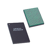
EP3C16F484I7N Altera, EP3C16F484I7N Datasheet - Page 209

EP3C16F484I7N
Manufacturer Part Number
EP3C16F484I7N
Description
Cyclone III
Manufacturer
Altera
Datasheet
1.EP3C16F484I7N.pdf
(274 pages)
Specifications of EP3C16F484I7N
Family Name
Cyclone III
Number Of Logic Blocks/elements
15408
# I/os (max)
346
Frequency (max)
437.5MHz
Process Technology
65nm
Operating Supply Voltage (typ)
1.2V
Logic Cells
15408
Ram Bits
516096
Operating Supply Voltage (min)
1.15V
Operating Supply Voltage (max)
1.25V
Operating Temp Range
-40C to 100C
Operating Temperature Classification
Industrial
Mounting
Surface Mount
Pin Count
484
Package Type
FBGA
Lead Free Status / Rohs Status
Compliant
Available stocks
Company
Part Number
Manufacturer
Quantity
Price
Company:
Part Number:
EP3C16F484I7N
Manufacturer:
ALTERA
Quantity:
4 000
Company:
Part Number:
EP3C16F484I7N
Manufacturer:
ALTERA41
Quantity:
60
Part Number:
EP3C16F484I7N
Manufacturer:
ALTERA/阿尔特拉
Quantity:
20 000
- Current page: 209 of 274
- Download datasheet (6Mb)
Chapter 9: Configuration, Design Security, and Remote System Upgrades in the Cyclone III Device Family
Configuration Features
Table 9–15. Dedicated JTAG Pins
© December 2009
TDI
TDO
TMS
TCK
Name
Pin
Test data input
Test data output
Test mode select
Test clock input
f
Pin Type
Altera Corporation
For more information about how to connect a JTAG chain with multiple voltages
across the devices in the chain, refer to the
for Cyclone III Devices
You can download data to the device on the PCB through the USB-Blaster,
MasterBlaster, ByteBlaster II, ByteBlasterMV download cable, and Ethernet-Blaster
communications cable during JTAG configuration. Configuring devices using a cable
is similar to programming devices in-system.
JTAG configuration of a single Cyclone III device family.
For device V
maintain a maximum AC voltage of 4.1 V. Because JTAG pins do not have the internal
PCI clamping diodes to prevent voltage overshoot when using V
3.3 V, you must power up the V
V
For device V
the download cabled with the supply from V
CCA
.
Serial input pin for instructions as well as test and programming data. Data shifts in on the
rising edge of
required on the board, the JTAG circuitry is disabled by connecting this pin to V
Serial data output pin for instructions as well as test and programming data. Data shifts out on
the falling edge of
TDO pin is powered by V
JTAG circuitry is disabled by leaving this pin unconnected.
Input pin that provides the control signal to determine the transitions of the TAP controller state
machine. Transitions in the state machine occur on the rising edge of
must be set up before the rising edge of
TMS pin is powered by the V
JTAG circuitry is disabled by connecting this pin to V
Clock input to the BST circuitry. Some operations occur at the rising edge while others occur at
the falling edge. The
required on the board, the JTAG circuitry is disabled by connecting this pin to GND.
CCIO
CCIO
of 1.2, 1.5, and 1.8 V, refer to
of 2.5, 3.0, and 3.3 V, refer to
TCK . The TDI pin is powered by the V
TCK . The pin is tri-stated if data is not being shifted out of the device. The
chapter.
TCK pin is powered by the V
CCIO
in I/O bank 1. If the JTAG interface is not required on the board, the
CCIO
CC
supply. If the JTAG interface is not required on the board, the
of the download cable with a 2.5-V supply from
TCK . TMS is evaluated on the rising edge of TCK . The
Description
IEEE 1149.1 (JTAG) Boundary-Scan Testing
Figure
Figure
CCIO
Figure 9–24
CCIO
.
CC
supply. If the JTAG interface is not
CCIO
.
9–25. You can power up the V
9–24. All I/O inputs must
supply. If the JTAG interface is not
Cyclone III Device Handbook, Volume 1
and
Figure 9–25
TCK . Therefore, TMS
CCIO
of 2.5, 3.0, and
CC
.
show the
CC
9–49
of
Related parts for EP3C16F484I7N
Image
Part Number
Description
Manufacturer
Datasheet
Request
R

Part Number:
Description:
CYCLONE II STARTER KIT EP2C20N
Manufacturer:
Altera
Datasheet:

Part Number:
Description:
CPLD, EP610 Family, ECMOS Process, 300 Gates, 16 Macro Cells, 16 Reg., 16 User I/Os, 5V Supply, 35 Speed Grade, 24DIP
Manufacturer:
Altera Corporation
Datasheet:

Part Number:
Description:
CPLD, EP610 Family, ECMOS Process, 300 Gates, 16 Macro Cells, 16 Reg., 16 User I/Os, 5V Supply, 15 Speed Grade, 24DIP
Manufacturer:
Altera Corporation
Datasheet:

Part Number:
Description:
Manufacturer:
Altera Corporation
Datasheet:

Part Number:
Description:
CPLD, EP610 Family, ECMOS Process, 300 Gates, 16 Macro Cells, 16 Reg., 16 User I/Os, 5V Supply, 30 Speed Grade, 24DIP
Manufacturer:
Altera Corporation
Datasheet:

Part Number:
Description:
High-performance, low-power erasable programmable logic devices with 8 macrocells, 10ns
Manufacturer:
Altera Corporation
Datasheet:

Part Number:
Description:
High-performance, low-power erasable programmable logic devices with 8 macrocells, 7ns
Manufacturer:
Altera Corporation
Datasheet:

Part Number:
Description:
Classic EPLD
Manufacturer:
Altera Corporation
Datasheet:

Part Number:
Description:
High-performance, low-power erasable programmable logic devices with 8 macrocells, 10ns
Manufacturer:
Altera Corporation
Datasheet:

Part Number:
Description:
Manufacturer:
Altera Corporation
Datasheet:

Part Number:
Description:
Manufacturer:
Altera Corporation
Datasheet:

Part Number:
Description:
Manufacturer:
Altera Corporation
Datasheet:

Part Number:
Description:
CPLD, EP610 Family, ECMOS Process, 300 Gates, 16 Macro Cells, 16 Reg., 16 User I/Os, 5V Supply, 25 Speed Grade, 24DIP
Manufacturer:
Altera Corporation
Datasheet:


