MT9T031C12STC Aptina LLC, MT9T031C12STC Datasheet
MT9T031C12STC
Specifications of MT9T031C12STC
Available stocks


Related parts for MT9T031C12STC


MT9T031C12STC Summary of contents
Page 1
... Operating temperature 0°C to 60°C Packaging 48-pin CLCC Ordering Information Table 2: Available Part Numbers Part Number MT9T031C12STC 48-Pin CLCC MT9T031C12STCD ES 48-Pin CLCC demo MT9T031C12STCH ES 48-Pin CLCC headboard 1 . Applications Typical Value − 3.6V (3.3V nominal) Description . ©2006 Aptina Imaging Corporation All rights reserved. ...
Page 2
Table of Contents Applications . . . . . . . . . . . . . . . . . . . . . . . . . . . . . . . . . . . . ...
Page 3
Revision History ...
Page 4
List of Figures Figure 1: Block Diagram . . . . . . . . . . . . . . . . . . . . . . . . . . . . . . . . . ...
Page 5
List of Tables Table 1: Key Performance Parameters ...
Page 6
General Description The sensor can be operated in its default mode or programmed by the user for frame size, exposure, gain setting, and other parameters. The default mode outputs a QXGA image at 12 frames per second (fps). An on-chip ...
Page 7
Figure 2: Typical Configuration (Connection) TWO-WIRE SERIAL BUS MASTER CLOCK 10µF Note: 1. Resistor value 1.5KΩ is recommended, but may be greater for slower two-wire speed. PDF: 3682685119/Source: 9830567334 MT9T031_DS - Rev.E 5/ 0.1µF 2.2µF D ...
Page 8
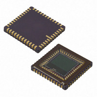
Figure 3: 48-Pin CLCC STANDBY TRIGGER RESET# GSHT_CTL OE# A GND V A GND A GND . Table 3: Pin Descriptions Pin Numbers Symbol 7 STANDBY 8 TRIGGER 10 RESET# 13 OE# 29 EXTCLK 46 SCLK 12 GSHT_CTL 45 S ...
Page 9
Table 3: Pin Descriptions (Continued) Pin Numbers Symbol 5, 23, 38 Supply GND 16 Supply AA 15, 17, 18, 21, A Supply GND 47 11,14,19, 30 42, 44 PDF: 3682685119/Source: ...
Page 10
Pixel Data Format Pixel Array Structure The MT9T031 pixel array is configured as 2,112 columns by 1,568 rows, as shown in Figure 4. Columns from 0 through 27 and from 2,085 through 2,111 are optically black. Similarly, rows from 0 ...
Page 11
Output Data Format The MT9T031 image data is read out in a progressive scan. Valid image data is surrounded by horizontal blanking and vertical blanking, as shown in Figure 6. The amount of horizontal blanking and vertical blanking is programmable ...
Page 12
Figure 8: Row Timing and FRAME_VALID/LINE_VALID Signals FRAME_VALID LINE_VALID Number of master clocks Frame Timing Formulas Table 4: Frame Timing Parameter Name R Active Rows A Active Columns P1 Frame Start Blanking 1 P2 Frame Start Blanking 2 P3 Frame ...
Page 13
Register List and Default Values Table 5: Core Registers *1 = always always programmable read only Register # Dec (Hex) Register Description R0(R0x00) R1(R0x01) R2(R0x02) R3(R0x03) R4(R0x04) R5(R0x05) Horizontal Blanking R6(R0x06) R7(R0x07) ...
Page 14
Table 5: Core Registers (Continued always always programmable read only Register # Dec (Hex) Register Description R74(R0x4A) R75(R0x4B) Row Black Default Offset R76(R0x4C) R77(R0x4D) R78(R0x4E) R79(R0x4F) R80(R0x50) R81(R0x51) R82(R0x52) R83(R0x53) ...
Page 15
Table 5: Core Registers (Continued always always programmable read only Register # Dec (Hex) Register Description R124(R0x7C) R125(R0x7D) R126(R0x7E) R127(R0x7F) R128(R0x80) R129(R0x81) R130(R0x82) R131(R0x83) R132(R0x84) R134(R0x86) R135(R0x87) R137(R0x89) R138(R0x8A) R139(R0x8B) ...
Page 16
Sensor Core Register Descriptions Table 6: Core Registers Reg. # Bits Default R0 15:0 0x1621 R0x00 Chip version. R1 15:0 0x0014 R0x01 The first row to be read out, excluding any dark rows that may be read. To window the ...
Page 17
Table 6: Core Registers (Continued) Reg. # Bits Default R8 15:0 0x0000 R0x08 The most significant bits of the shutter width, which are combined with Shutter Width (R0x09). The total shutter width is therefore: (((Shutter_Width_Upper) x 65536) + Shutter_Width). This ...
Page 18
Table 6: Core Registers (Continued) Reg. # Bits Default R30 10 0x0000 R0x1E 9 0x0000 8 0x0000 7 0x0000 6 0x0001 5:0 0x0000 R32 15:0 0x2000 R0x20 15 0x0000 14 0x0000 13 0x0001 12 0x0000 11 0x0000 10 0x0000 9 ...
Page 19
Table 6: Core Registers (Continued) Reg. # Bits Default R34 15:0 0x0000 R0x22 15 X 14:12 0x0000 11 X 10:8 0x0000 7 X 6:4 0x0000 3 X 2:0 0x0000 R35 15:0 0x0000 R0x23 15:11 X 10:8 0x0000 7:6 X 5:4 ...
Page 20
Table 6: Core Registers (Continued) Reg. # Bits Default R45 15:0 0x0008 R0x2D 15 X 14:8 0x0000 0x0000 5:0 0x0008 R46 15:0 0x0008 R0x2E 15 X 14:8 0x0000 0x0000 5:0 0x0008 R50 15:0 0x0000 ...
Page 21
Table 6: Core Registers (Continued) Reg. # Bits Default R95 15:0 0x231D R0x5F 15 X 14:8 0x0023 7 X 6:0 0x001D R96 15:0 0x0020 R0x60 Analog calibration offset for green1 pixels, represented as a two’s complement signed 8-bit value (if ...
Page 22
Table 6: Core Registers (Continued) Reg. # Bits Default R99 15:0 0x0020 R0x63 Analog calibration offset for red pixels, represented as a two’s complement signed 8-bit value (if bit 8 is clear, the offset is positive and the magnitude is ...
Page 23
Feature Description Window Control R0x01, R0x02, R0x03, and R0x04 These registers control the size of the window. Window Size The default programmed window size is 2,048 columns by 1,536 rows (2,048H x 1,536V). The control logic allows the flexibility to ...
Page 24
Electronic Panning In addition to changing the window size, the user has the flexibility to change the loca- tion of the readout window. R0x01 controls the first row to be read out and R0x02 controls the first column to be ...
Page 25
Figure 9: Windowing Capabilities (2048, 1536) Window A Window B Window C Window D Table 9: Auto Focus Modes Column_ Resolu- Frame Size tion Rate (R0 04) x 2,048 x 512 30 fps 2,047 2,048 x 256 60 fps 2,047 ...
Page 26
Pixel Integration Time Control R0x09 and R0x0C The integration time of the pixel is the amount of time the pixels are set to collect charge generated from light. The user can change the integration time of the sensor by programming ...
Page 27
Strobe Pulse Output The STROBE pulse must be enabled before use by setting R0x1E [bit The STROBE signal has two options for pulse length and may be selected using R0x1E [bit 10] as shown in Table 10. ...
Page 28
Bulb Mode To use bulb mode: 1. Set up snapshot mode as normal (including any STROBE preferences). 2. Set R0x21 (Read Mode 3) to 0x0001. 3. Assert (transition LOW to HIGH) the GSHT_CTL pin. 4. Assert (transition LOW to HIGH) ...
Page 29
Table 12: Skip and Bin Modes Register Bit R0x23 Bit[2–0] No column skip Column skip 2X Column skip 3X Column skip 4X Column skip 8X Bit[5–4] Column Bin 2X Column Bin 3X R0x22 Bit[2–0] No row skip Row skip 2X ...
Page 30
Figure 12: Column Skip 3X; Row Skip 3X Enabled ...
Page 31
Figure 13: Column Skip 4X; Row Skip 4X Enabled ... ...
Page 32
Figure 15: Bin 2-to-1: 2,048H x 1,536V (QXGA) to 1,024H x 768V (XGA Note: Grs = binning of 4 Gr[ window; Gbs = binning of 4 Gb[ ...
Page 33
If the user sets R0x03 = 0x02FF (768V rows), R0x04 = 0x03FF (1,024H columns), and then enable column skip 2X and row skip 2X, the effective readout resolution is 512H x 384V. Line_Valid Formats R0x20 is used to control many ...
Page 34
Signal Path The MT9T031 sensor analog signal path consists of the pixel array, the column sample and hold (S/H) circuitry, the programmable gain stage, the analog offset correction and the analog-to-digital converter (ADC). The reset and signal voltages from the ...
Page 35
Gain Settings R0x2B, R0x2C, R0x2D, R0x2E, and R0x35 The analog programmable gain stage consists of two stages of gain circuitry that operate in a pipelined manner. The first stage of gain has programmable gain while the ...
Page 36
Analog offset = Bit[8: LSB The 1 LSB value in the formula is an estimate amount. It deviates from 1 LSB with process variation. Black Level R0x49 Digital offset is applied such that the average black level of ...
Page 37
Sequence A typical read or write sequence begins by the master sending a start bit. After the start bit, the master sends the slave device's 8-bit address. The last bit of the address deter- mines if the request is a ...
Page 38
Acknowledge Bit The master generates the acknowledge clock pulse. The transmitter (which is the master when writing, or the slave when reading) releases the data line, and the receiver indi- cates an acknowledge bit by pulling the data line LOW ...
Page 39
Two-Wire Serial Interface Sample Write and Read Sequences 16-Bit Write Sequence A typical write sequence for writing 16 bits to a register is shown in Figure 19. A start bit given by the master, followed by the write address, starts ...
Page 40
Electrical Specifications Two-Wire Serial Register Interface The electrical characteristics of the two-wire serial register interface (SCLK, S shown in Figure 21 and Table 14 on page 41. Figure 21: Two-Wire Serial Bus Timing Parameters t SRTH t SCLK SCLK S ...
Page 41
Table 14: Two-Wire Serial Bus Characteristics Symbol Definition f SCLK Serial interface input clock frequency t SCLK Serial Input clock period SCLK Duty Cycle tr_sclk SCLK rise time tf_sclk SCLK fall time tr_sdat S rise time DATA tf_sdat S fall ...
Page 42
Table 15: I/O Timing Characteristics Symbol Definition f EXTCLK1 Input clock frequency t EXTCLK1 Input clock period t R Input clock rising edge slew rate t F Input clock falling edge slew rate t RP Pixclk rising edge slew rate ...
Page 43
Table 17: Absolute Maximum Ratings Symbol V _MAX Core digital voltage DD V _MAX Analog voltage AA V PIX_MAX Pixel supply voltage AA V _MAX Input voltage IN I _MAX Digital operating current DD I _MAX Analog operating current AA ...
Page 44
Figure 23: Quantum Efficiency Note: Diagram not to scale. Figure 24: Image Center Offset 7.721mm Note: Diagram not to scale. PDF: 3682685119/Source: 9830567334 MT9T031_DS - Rev.E 5/11 EN Quantum Efficiency 350 ...
Page 45
Figure 25: 48-Pin CLCC Note: All dimensions in millimeters. PDF: 3682685119/Source: 9830567334 MT9T031_DS - Rev.E 5/11 EN MT9T031: 1/2-Inch 3-Mp Digital Image Sensor 45 Electrical Specifications ©2006 Aptina Imaging Corporation All rights reserved. ...
Page 46
Revision History Rev ...