MT9T031C12STC Aptina LLC, MT9T031C12STC Datasheet - Page 8
MT9T031C12STC
Manufacturer Part Number
MT9T031C12STC
Description
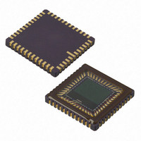
IC SENSOR IMAGE COLOR 48CLCC
Manufacturer
Aptina LLC
Series
Micron®DigitalClarity®r
Type
CMOS Imagingr
Datasheets
1.MT9T031C12STCH_ES.pdf
(12 pages)
2.MT9T031C12STCH_ES.pdf
(2 pages)
3.MT9T031C12STC.pdf
(2 pages)
4.MT9T031C12STC.pdf
(46 pages)
Specifications of MT9T031C12STC
Pixel Size
3.2µm x 3.2µm
Active Pixel Array
2048H x 1536V
Frames Per Second
12 ~ 93
Voltage - Supply
3 V ~ 3.6 V
Package / Case
48-CLCC
Brief Features
Superior Low Light Performance, Programmable Controls, Low Dark Current, High Frame Rate
Supply Voltage Range
3V To 3.6V
Operating Temperature Range
0°C To +60°C
Ic Function
Digital Image Sensor
Lead Free Status / RoHS Status
Lead free / RoHS Compliant
For Use With
557-1450 - KIT HEAD BOARD FOR MT9T031557-1451 - KIT DEV FOR MT9T031
Lead Free Status / Rohs Status
Compliant
Other names
557-1452
Available stocks
Company
Part Number
Manufacturer
Quantity
Price

Part Number:
MT9T031C12STC
Manufacturer:
APTINA
Quantity:
20 000


Figure 3:
Table 3:
PDF: 3682685119/Source: 9830567334
MT9T031_DS - Rev.E 5/11 EN
24, 25, 26, 27,
28, 32, 33, 34,
Pin Numbers
4, 22, 37
35, 36
10
13
29
46
12
45
31
39
40
41
7
8
1
Pin Descriptions
48-Pin CLCC
FRAME_VALID
LINE_VALID
GSHT_CTL
STANDBY
D
TRIGGER
STROBE
Symbol
EXTCLK
VAAPIX
RESET#
PIXCLK
OUT
S
SCLK
OE#
V
DATA
DD
[9:0]
GSHT_CTL
STANDBY
.
TRIGGER
RESET#
A
A
A
Output
Output
Output
Output
Output
OE#
Supply
Supply
V
GND
GND
GND
Input
Input
Input
Input
Input
Input
Input
Type
NC
NC
NC
AA
I/O
10
11
12
14
15
16
17
18
13
7
8
9
19
6
Description
Standby: activates (HIGH) standby mode, disables analog bias circuitry for power saving
mode.
Trigger: activates (HIGH) snapshot sequence.
Reset: activates (LOW) asynchronous reset of sensor. All registers assume factory defaults.
Output enable: OE# when HIGH, places outputs D
PIXCLK, and STROBE into a tri-state configuration.
Clock in: master clock into sensor (48 MHz maximum).
Serial clock: clock for serial interface.
Global shutter control.
Serial data: serial data bus, requires 1.5
Data out: pixel data output bit 0, D
Pixel clock: pixel data outputs are valid during falling edge of this clock. Frequency =
(master clock).
Strobe: output is pulsed HIGH to indicate sensor reset operation of pixel array has
completed.
Line valid: output is pulsed HIGH during line of selectable valid pixel data (see R0x20 for
options).
Frame valid: output is pulsed HIGH during frame of valid pixel data.
Analog pixel power: provide power supply for pixel array, 3.3V ±0.3V.
Digital power: provide power supply for digital block, 3.3V ±0.3V.
20
5
21
4
22
3
23
2
24
1
8
48
25
47
26
46
MT9T031: 1/2-Inch 3-Mp Digital Image Sensor
27
28
45
OUT
[9] (MSB), D
44
29
KΩ
30
43
resistor to 3.3V for pull-up.
42
41
40
39
38
37
36
35
34
33
32
31
NC
FRAME_VALID
LINE_VALID
STROBE
D
V
D
D
D
D
D
PIXCLK
OUT
DD
GND
OUT
OUT
OUT
OUT
OUT
OUT
[9:0], FRAME_VALID, LINE_VALID,
[9]
[8]
[7]
[6]
[5]
[0] (LSB).
©2006 Aptina Imaging Corporation. All rights reserved.
General Description
Related parts for MT9T031C12STC
Image
Part Number
Description
Manufacturer
Datasheet
Request
R

Part Number:
Description:
SENSOR IMAGE VGA COLOR CMOS PLCC
Manufacturer:
Aptina LLC
Datasheet:

Part Number:
Description:
SENSOR IMAGE 1.3MP CMOS 48-CLCC
Manufacturer:
Aptina LLC
Datasheet:

Part Number:
Description:
SENSOR IMAGE 2MP CMOS 48-CLCC
Manufacturer:
Aptina LLC
Datasheet:

Part Number:
Description:
SENSOR IMAGE VGA MONO 52IBGA
Manufacturer:
Aptina LLC
Datasheet:

Part Number:
Description:
SENSOR IMAGE VGA COLOR 48CLCC
Manufacturer:
Aptina LLC
Datasheet:

Part Number:
Description:
SENSOR IMAGE COLOR CMOS 48-PLCC
Manufacturer:
Aptina LLC
Datasheet:

Part Number:
Description:
KIT HEAD BOARD FOR MT9P031
Manufacturer:
Aptina LLC
Datasheet:

Part Number:
Description:
KIT HEAD BOARD FOR MT9D131
Manufacturer:
Aptina LLC
Datasheet:

Part Number:
Description:
KIT HEAD BOARD FOR MT9P031
Manufacturer:
Aptina LLC
Datasheet:

Part Number:
Description:
KIT HEAD BOARD FOR MT9M032
Manufacturer:
Aptina LLC
Datasheet:

Part Number:
Description:
PARALLEL HEADBOARD FOR MT9M032
Manufacturer:
Aptina LLC
Datasheet:
Part Number:
Description:
SENSOR IMAGE VGA COLOR CMOS PLCC
Manufacturer:
Aptina LLC
Datasheet:
Part Number:
Description:
SENSOR IMAGE 2MP CMOS 48-CLCC
Manufacturer:
Aptina LLC
Datasheet:
