STGW39NC60VD STMicroelectronics, STGW39NC60VD Datasheet
STGW39NC60VD
Specifications of STGW39NC60VD
Available stocks


Related parts for STGW39NC60VD


STGW39NC60VD Summary of contents
Page 1
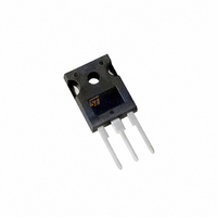
... This IGBT utilizes the advanced PowerMESH™ process resulting in an excellent trade-off between switching performance and low on-state behavior. Table 1. Device summary Order code STGW39NC60VD July 2008 600 V - very fast IGBT Figure 1. Marking Package GW39NC60VD TO-247 Rev 8 STGW39NC60VD TO-247 Internal schematic diagram Packaging Tube www.st.com 1/15 15 ...
Page 2
... Contents Contents 1 Electrical ratings . . . . . . . . . . . . . . . . . . . . . . . . . . . . . . . . . . . . . . . . . . . . 3 2 Electrical characteristics . . . . . . . . . . . . . . . . . . . . . . . . . . . . . . . . . . . . . 4 2.1 Electrical characteristics (curves) 2.2 Frequency applications . . . . . . . . . . . . . . . . . . . . . . . . . . . . . . . . . . . . . . . 9 3 Test circuit . . . . . . . . . . . . . . . . . . . . . . . . . . . . . . . . . . . . . . . . . . . . . . . 10 4 Package mechanical data . . . . . . . . . . . . . . . . . . . . . . . . . . . . . . . . . . . . 11 5 Revision history . . . . . . . . . . . . . . . . . . . . . . . . . . . . . . . . . . . . . . . . . . . 13 2/15 STGW39NC60VD . . . . . . . . . . . . . . . . . . . . . . . . . . . 6 ...
Page 3
... STGW39NC60VD 1 Electrical ratings Table 2. Absolute maximum ratings Symbol V Collector-emitter voltage (V CES (1) Collector current (continuous ° (1) Collector current (continuous) at 100 ° (2) Turn-off latching current I CL (3) Pulsed collector current Gate-emitter voltage GE I Diode RMS forward current Surge non repetitive forward current I FSM (tp=10 ms sinusoidal) ...
Page 4
... Gate-emitter charge ge Gate-collector charge Q gc 4/15 Parameter Test conditions =125 ° 600 600 ± Parameter Test conditions MHz 390 (see Figure 19) STGW39NC60VD Min. Typ. Max. Unit 600 = 125 ° Min. Typ. Max. Unit 2900 = 0 298 126 2 5.75 V 500 µ ±100 ...
Page 5
... STGW39NC60VD Table 6. Switching on/off (inductive load) Symbol t Turn-on delay time d(on) t Current rise time r Turn-on current slope (di/dt) onf t Turn-on delay time d(on) t Current rise time r Turn-on current slope (di/dt Off voltage rise time r(Voff) t Turn-off delay time d(off) Current fall time ...
Page 6
... Reverse recovery current I rrm t Reverse recovery time rr Q Reverse recovery charge rr Reverse recovery current I rrm 6/15 Parameter Test conditions di/dt =100 A/µs (see Figure 21 125 °C, C di/dt =100 A/µs (see Figure 21) STGW39NC60VD Min. Typ. Max. 2.4 = 125 ° 100 290 5.8 Unit ...
Page 7
... STGW39NC60VD 2.1 Electrical characteristics (curves) Figure 2. Output characteristics Figure 4. Transconductance Figure 6. Collector-emitter on voltage vs collector current Electrical characteristics Figure 3. Transfer characteristics Figure 5. Collector-emitter on voltage vs temperature Figure 7. Normalized gate threshold vs temperature 7/15 ...
Page 8
... Electrical characteristics Figure 8. Normalized breakdown voltage vs temperature Figure 10. Capacitance variations Figure 12. Switching losses vs gate resistance Figure 13. Switching losses vs collector 8/15 Figure 9. Gate charge vs gate-emitter voltage Figure 11. Switching losses vs temperature current STGW39NC60VD ...
Page 9
... STGW39NC60VD Figure 14. Thermal impedance Figure 16. Emitter-collector diode characteristics IFM(A) 120 110 Tj=125°C Tj=125°C (Maximum values) (Maximum values) 100 90 80 Tj=125°C Tj=125°C 70 (Typical values) (Typical values VFM( 2.2 Frequency applications For a fast IGBT suitable for high frequency applications, the typical collector current vs. ...
Page 10
... included in the E ON measurements (see note 3). 10/15 * δ typical value @125 °C. CESAT ) * freq.Typical values @ 125 °C for switching losses are used (test = 10 Ω). Furthermore, diode recovery energy (see note 2), while the tail of the collector current is included in the E STGW39NC60VD OFF ...
Page 11
... STGW39NC60VD 3 Test circuit Figure 18. Test circuit for inductive load switching Figure 20. Switching waveforms Figure 19. Gate charge test circuit Figure 21. Diode recovery times waveform Test circuit 11/15 ...
Page 12
... These packages have a lead-free second level interconnect. The category of second level interconnect is marked on the package and on the inner box label, in compliance with JEDEC Standard JESD97. The maximum ratings related to soldering conditions are also marked on the inner box label. ECOPACK trademark. ECOPACK specifications are available at: 12/15 www.st.com STGW39NC60VD ...
Page 13
... STGW39NC60VD Dim øP øR S TO-247 mechanical data mm. Min. Typ 4.85 2.20 1.0 2.0 3.0 0.40 19.85 15.45 5.45 14.20 3.70 18.50 3.55 4.50 5.50 Package mechanical data Max . 5.15 2.60 1.40 2.40 3.40 0.80 20.15 15.75 14.80 4.30 3.65 5.50 13/15 ...
Page 14
... Revision 1 First release 2 Inserted curves Absolute maximum ratings 3 Modified value on Dynamic 4 Modified value on updated:Figure 5 5 New curves Figure 17 Added new 6 applications Table 8: Collector-emitter diode 7 Modified: 8 Updated V on CE(sat) STGW39NC60VD Changes Figure 6 and 2.2: Frequency and new section Table 4 ...
Page 15
... STGW39NC60VD Information in this document is provided solely in connection with ST products. STMicroelectronics NV and its subsidiaries (“ST”) reserve the right to make changes, corrections, modifications or improvements, to this document, and the products and services described herein at any time, without notice. All ST products are sold pursuant to ST’s terms and conditions of sale. ...