UDA1341TSDB NXP Semiconductors, UDA1341TSDB Datasheet
UDA1341TSDB
Specifications of UDA1341TSDB


Related parts for UDA1341TSDB


UDA1341TSDB Summary of contents
Page 1
DATA SHEET UDA1341TS Economy audio CODEC for MiniDisc (MD) home stereo and portable applications Product specification Supersedes data of 2001 Jun 29 INTEGRATED CIRCUITS 2002 May 16 ...
Page 2
... NXP Semiconductors Economy audio CODEC for MiniDisc (MD) home stereo and portable applications CONTENTS 1 FEATURES 1.1 General 1.2 Multiple format data interface 1.3 DAC digital sound processing 1.4 Advanced audio configuration 2 GENERAL DESCRIPTION 3 ORDERING INFORMATION 4 QUICK REFERENCE DATA 5 BLOCK DIAGRAM 6 PINNING 7 FUNCTIONAL DESCRIPTION 7 ...
Page 3
... NXP Semiconductors Economy audio CODEC for MiniDisc (MD) home stereo and portable applications 1 FEATURES 1.1 General • Low power consumption • 3.0 V power supply • 256f , 384f or 512f system clock frequencies ( • Small package size (SSOP28) • Partially pin compatible with UDA1340M and UDA1344TS • ...
Page 4
... NXP Semiconductors Economy audio CODEC for MiniDisc (MD) home stereo and portable applications 4 QUICK REFERENCE DATA SYMBOL PARAMETER Supplies V ADC analog supply voltage DDA(ADC) V DAC analog supply voltage DDA(DAC) V digital supply voltage DDD I ADC analog supply current DDA(ADC) I DAC analog supply current ...
Page 5
... NXP Semiconductors Economy audio CODEC for MiniDisc (MD) home stereo and portable applications 5 BLOCK DIAGRAM V DDA(ADC) handbook, full pagewidth 6 VINL2 2 VINL1 18 DATAO 16 BCK DATAI 23 QMUTE 28 V ref 26 VOUTL V DDA(DAC) 2002 May 16 V SSA(ADC) V DDD V SSD PGA ADC2 ADC2 0 dB/6 dB SWITCH ADC1 UDA1341TS ...
Page 6
... NXP Semiconductors Economy audio CODEC for MiniDisc (MD) home stereo and portable applications 6 PINNING SYMBOL PIN V 1 ADC analog ground SSA(ADC) VINL1 2 ADC1 input left V 3 ADC analog supply voltage DDA(ADC) VINR1 4 ADC1 input right V 5 ADC negative reference voltage ADCN VINL2 ...
Page 7
... NXP Semiconductors Economy audio CODEC for MiniDisc (MD) home stereo and portable applications 7 FUNCTIONAL DESCRIPTION 7.1 System clock The UDA1341TS accommodates slave mode only, this means that in all applications the system devices must provide the system clock. The system frequency is selectable. The options are 256f The system clock must be locked in frequency to the digital interface signals ...
Page 8
... NXP Semiconductors Economy audio CODEC for MiniDisc (MD) home stereo and portable applications 7.9 Decimation filter (ADC) The decimation from 128f is performed in two stages. s The first stage realizes 3rd order decimating by 16. The second stage consists of 3 half-band filters, each decimating by a factor of 2. ...
Page 9
... NXP Semiconductors Economy audio CODEC for MiniDisc (MD) home stereo and portable applications 7.16 Filter Stream Digital-to-Analog Converter (FSDAC) The FSDAC is a semi-digital reconstruction filter that converts the 1-bit data stream of the noise shaper to an analog output voltage. The filter coefficients are implemented as current sources and are summed at virtual ground of the output operational amplifier ...
Page 10
WS LEFT >= BCK DATA MSB B2 LSB WS LEFT >= BCK DATA MSB B2 LSB MSB WS LEFT 16 BCK DATA MSB WS LEFT BCK DATA MSB B2 ...
Page 11
... NXP Semiconductors Economy audio CODEC for MiniDisc (MD) home stereo and portable applications 7.18 L3-interface The UDA1341TS has a microcontroller input mode. In the microcontroller mode, all the digital sound processing features and the system controlling features can be controlled by the microcontroller. The controllable features are: • ...
Page 12
... NXP Semiconductors Economy audio CODEC for MiniDisc (MD) home stereo and portable applications Table 4 Selection of data transfer BIT 1 BIT 0 MODE 0 0 DATA0 direct addressing registers: volume, bass boost, treble, peak detection position, de-emphasis, mute and mode extended addressing registers: digital mixer control, AGC control, MIC sensitivity control, ...
Page 13
... NXP Semiconductors Economy audio CODEC for MiniDisc (MD) home stereo and portable applications t stp(L3) handbook, full pagewidth L3MODE t su(L3)D L3CLOCK L3DATA write L3DATA read handbook, full pagewidth L3MODE L3CLOCK L3DATA 2002 May 16 t CLK(L3)L T cy(CLK)L3 t CLK(L3)H t h(L3)DA t su(L3)DA BIT 0 PL0 PL1 PL2 PL3 Fig ...
Page 14
... NXP Semiconductors Economy audio CODEC for MiniDisc (MD) home stereo and portable applications 7.21 Programming the sound processing and other features The sound processing and other feature values are stored in independent registers. The first selection of the registers is achieved by the choice of data type that is transferred. This is performed in the address mode using bit 0 and bit 1 (see Table 4) ...
Page 15
... NXP Semiconductors Economy audio CODEC for MiniDisc (MD) home stereo and portable applications 7.21.1 STATUS CONTROL Table 6 Data transfer of type ‘STATUS’ BIT 7 BIT 6 BIT 5 BIT 4 BIT 3 BIT 2 BIT 1 BIT 0 0 RST SC1 SC0 IF2 1 OGS IGS PAD PDA 7.21.1.1 Reset A 1-bit value to initialize the L3-registers with the default settings except system clock frequency ...
Page 16
... NXP Semiconductors Economy audio CODEC for MiniDisc (MD) home stereo and portable applications 7.21.1.5 Output gain switch A 1-bit value to control the DAC output gain switch. The default setting is given in Table 5. Table 11 Gain switch of DAC settings OGS GAIN OF DAC 7.21.1.6 Input gain switch A 1-bit value to control the ADC input gain switch ...
Page 17
... NXP Semiconductors Economy audio CODEC for MiniDisc (MD) home stereo and portable applications 7.21.2 DATA0 DIRECT CONTROL Table 17 Data transfer of type ‘DATA0’ BIT 7 BIT 6 BIT 5 BIT 4 BIT 3 BIT 2 BIT 1 BIT VC5 VC4 VC3 0 1 BB3 BB2 BB1 DE1 DE0 ED4 ED3 7 ...
Page 18
... NXP Semiconductors Economy audio CODEC for MiniDisc (MD) home stereo and portable applications 7.21.2.3 Treble A 2-bit value to program the treble setting. The used set depends on the mode bits. The default setting is given in Table 5. Table 20 Treble settings TR1 TR0 FLAT (dB 7.21.2.4 Peak detection position A 1-bit value to control the position of the peak level detector in the signal processing path ...
Page 19
... NXP Semiconductors Economy audio CODEC for MiniDisc (MD) home stereo and portable applications 7.21.3 DATA0 EXTENDED PROGRAMMING REGISTERS Table 25 Extended control registers EA2 EA1 EA0 ED4 ED3 MA4 MA3 MA2 MA1 MA0 MA = mixer gain channel 1 (5 bits MB4 MB3 MB2 MB1 MB0 MB = mixer gain channel 2 (5 bits) ...
Page 20
... NXP Semiconductors Economy audio CODEC for MiniDisc (MD) home stereo and portable applications 7.21.3.3 Mixer mode A 2-bit value to program the mode of the digital mixer. There are four modes: double differential, input channel 1 select, input channel 2 select and digital mixer mode. The default setting is given in Table 5. ...
Page 21
... NXP Semiconductors Economy audio CODEC for MiniDisc (MD) home stereo and portable applications 7.21.4 DATA1 CONTROL Table 33 Data transfer of type ‘DATA1’ BIT 5 BIT 4 BIT 3 BIT 2 BIT 1 BIT 0 PL5 PL4 PL3 PL2 PL1 7.21.4.1 Peak level value A 6-bit value to indicate the peak level value of the playback data. The largest value of the left and right channel data in the playback signal path is held since the last read-out of the microcontroller ...
Page 22
... NXP Semiconductors Economy audio CODEC for MiniDisc (MD) home stereo and portable applications 8 LIMITING VALUES In accordance with the Absolute Maximum Rating System (IEC 60134 °C; unless otherwise specified. respect to ground; T amb SYMBOL PARAMETER V supply voltage DD T maximum crystal temperature xtal(max) T storage temperature ...
Page 23
... NXP Semiconductors Economy audio CODEC for MiniDisc (MD) home stereo and portable applications SYMBOL PARAMETER Digital input pins V HIGH-level input voltage IH V LOW-level input voltage input leakage current LI C input capacitance i Digital output pins V HIGH-level output voltage OH V LOW-level output voltage OL Analog-to-digital converter ...
Page 24
... NXP Semiconductors Economy audio CODEC for MiniDisc (MD) home stereo and portable applications 11 AC CHARACTERISTICS (ANALOG kHz; f DDD DDA i s (pins 1, 11 and 27); unless otherwise specified SYMBOL PARAMETER Analog-to-digital converter V input voltage (RMS value) i(rms) Δ V unbalance between i channels (THD + N)/S total harmonic ...
Page 25
... NXP Semiconductors Economy audio CODEC for MiniDisc (MD) home stereo and portable applications SYMBOL PARAMETER (THD + N)/S total harmonic distortion-plus-noise to signal ratio Digital-to-analog converter V output voltage (RMS value) note 3 o(rms) Δ V unbalance between o channels (THD + N)/S total harmonic distortion-plus-noise to signal ratio S/N signal-to-noise ratio α ...
Page 26
... NXP Semiconductors Economy audio CODEC for MiniDisc (MD) home stereo and portable applications 12 AC CHARACTERISTICS (DIGITAL 2 DDD DDA amb unless otherwise specified. SYMBOL PARAMETER System clock timing (see Fig.8) T clock cycle time sys t LOW-level pulse width CWL t HIGH-level pulse width CWH Serial input/output data timing (see Fig ...
Page 27
... NXP Semiconductors Economy audio CODEC for MiniDisc (MD) home stereo and portable applications t CWH handbook, full pagewidth T sys handbook, full pagewidth WS t BCK( BCK T cy DATAO DATAI 2002 May 16 t CWL Fig.8 System clock timing. t h; d(DATO)(WS) t BCK(L) Fig.9 Serial interface timing. ...
Page 28
... NXP Semiconductors Economy audio CODEC for MiniDisc (MD) home stereo and portable applications 13 APPLICATION INFORMATION L1 handbook, full pagewidth +3 V BLM32A07 L2 BLM32A07 C12 100 μF 100 μF ground (16 V) (16 V) R30 system clock 47 Ω overflow flag C1 left 47 μF line input ( right 47 μF (16 V) ...
Page 29
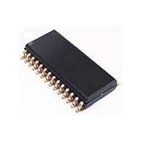
... NXP Semiconductors Economy audio CODEC for MiniDisc (MD) home stereo and portable applications 14 PACKAGE OUTLINE SSOP28: plastic shrink small outline package; 28 leads; body width 5 pin 1 index 1 e DIMENSIONS (mm are the original dimensions) A UNIT max. 0.21 1. 0.25 0.05 1.65 Note 1. Plastic or metal protrusions of 0.2 mm maximum per side are not included. ...
Page 30
... NXP Semiconductors Economy audio CODEC for MiniDisc (MD) home stereo and portable applications 15 SOLDERING 15.1 Introduction to soldering surface mount packages This text gives a very brief insight to a complex technology. A more in-depth account of soldering ICs can be found in our “Data Handbook IC26; Integrated Circuit Packages” ...
Page 31
... Notes 1. For more detailed information on the BGA packages refer to the “(LF)BGA Application Note” (AN01026); order a copy from your NXP Semiconductors sales office. 2. All surface mount (SMD) packages are moisture sensitive. Depending upon the moisture content, the maximum temperature (with respect to time) and body size of the package, there is a risk that internal or external package cracks may occur due to vaporization of the moisture in them (the so called popcorn effect). For details, refer to the Drypack information in the “ ...
Page 32
... In no event shall NXP Semiconductors be liable for any indirect, incidental, punitive, special or consequential damages (including - without limitation - lost profits, lost savings, business interruption, costs related to the ...
Page 33
... NXP Semiconductors’ specifications such use shall be solely at customer’s own risk, and (c) customer fully indemnifies NXP Semiconductors for any liability, damages or failed product claims resulting from customer design and use of the product for automotive applications beyond NXP Semiconductors’ ...
Page 34
... Interface, Security and Digital Processing expertise Customer notification This data sheet was changed to reflect the new company name NXP Semiconductors, including new legal definitions and disclaimers. No changes were made to the technical content, except for package outline drawings which were updated to the latest version. ...