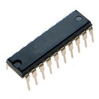
ETC5067N/C STMicroelectronics, ETC5067N/C Datasheet - Page 5

ETC5067N/C
Manufacturer Part Number
ETC5067N/C
Description
Telecom ICs Interfc CODEC Filter
Manufacturer
STMicroelectronics
Type
Telecom ICs - Variousr
Datasheet
1.ETC5064DC013TR.pdf
(18 pages)
Specifications of ETC5067N/C
Operating Supply Voltage
7 V
Operating Temperature Range
- 25 C to + 125 C
Mounting Style
Through Hole
Operating Frequency
2.048 MHz
Package / Case
PDIP-20
Lead Free Status / RoHS Status
Lead free / RoHS Compliant
Available stocks
Company
Part Number
Manufacturer
Quantity
Price
Part Number:
ETC5067N/C
Manufacturer:
ST
Quantity:
20 000
pulses are being used. For 64 kHz operation, the
frame sync pulses must be kept low for a minimum
of 160 ns (see Fig 1). The D
buffer is enabled with the rising edge of FS
rising edge of BCLK
the first bit clocked out is the sign bit. The following
seven BCLK
seven bits. The D
BCLK
FS
on the receive frame sync pulse, FS
PCM data at D
falling edges of BCLK
mode). Both devices may utilize the long frame sync
pulse in synchronous or asynchronous mode.
TRANSMIT SECTION
The transmit section input is an operational amplifier
with provision for gain adjustment using two external
resistors, see figure 4. The low noise and wide band-
width allow gains in excess of 20 dB across the
audio passband to be realized. The op amp drives
a unity gain filter consisting of RC active pre-filter,
followed by an eighth order switched-capacitor
bandpass filter directly drives the encoder sample-
and-hold circuit. The A/D is of companding type ac-
cording to A-law (ETC5067 and ETC5067-X) or -
law (ETC5064 and ETC5064-X) coding conven-
tions. A precision voltage reference is trimmed in
manufacturing to provide an input over load (t
of nominally 2.5V peak (see table of Transmission
Characteristics). The FS
the sampling of the filer output, and then the succes-
sive-approximation encoding cycle begins. The 8-bit
code is then loaded into a buffer and shifted out
through D
delay will be approximately 165 s (due to the trans-
mit filter) plus 125 s (due to encoding delay), which
totals 290 s. Any offset voltage due to the filters or
comparator is cancelled by sign bit integration.
ABSOLUTE MAXIMUM RATINGS
V
Symbol
X
IN
T
V
V
T
going low, whichever comes later. A rising edge
, V
oper
CC
stg
BB
X
OUT
edge following the eighth rising edge, or by
X
at the next FS
X
V
V
Voltage at any Analog Input or Output
Voltage at any Digital Input or Output
Operating Temperature Range: ETC5064/67
Storage Temperature Range
Lead Temperature (soldering, 10 seconds)
CC
BB
rising edges clock out the remaining
R
to GNDA
to GNDA
to be latched in on the next eight
X
output is disabled by the falling
X
, whichever comes later, and
R
X
X
frame sync pulse controls
(BCLK
pulse. the total encoding
X
TRI-STATE output
x
in synchronous
R
, will cause the
Parameter
ETC5064-X/67-X
X
or the
MAX
ETC5064 - ETC5064-X - ETC5067 - ETC5067-X
)
RECEIVE SECTION
The receive section consist of an expanding DAC
which drives a fifth order switched-capacitor low
pass filter clocked at 256kHz. The decoder is A-law
(ETC5067 and ETC5067-X) or –law (ETC5064
and ETC5064-X) and the 5 th order low pass filter
corrects for the sin x/x attenuation due to the 8kHz
sample and hold. The filter is then followed by a 2
nd order RC active post-filter and power amplifier
capable of driving a 600 load to a level of 7.2dBm.
The receive section is unity-gain. Upon the oc-
curence of FS
in on the falling edge of the next eight BCLK
(BCKL
the decoding cycle begins, and 10 s later the de-
coder DAC output is updated. The total decoder de-
lay is about10 s (decoder up-date) plus 110 s (fil-
ter delay) plus 62.5 s (1/2 frame), which gives ap-
proximately 180 s.
RECEIVE POWER AMPLIFIERS
Two inverting mode power amplifiers are provided
for directly driving a matched line interface trans-
former. The gain of the first power amplifier can be
adjusted to boost the 2.5V peak output signal from
the receive filter up 3.3V peak into an unbalanced
300 load, or 4.0V into an unbalanced 15k load.
The second power amplifier is internally connected
in unity-gain inverting mode to give 6dB of signal
gain for balanced loads. Maximum power transfer to
a 600
differientially driving a balanced transformer with a
power of 15.6dBm can be delivered to the load plus
termination. Both power amplifier can be powered
down independently from the PDN input by connect-
ing the VPI input to V
mW of power.
2
: 1 turns ratio, as shown in figure 4. A total peak
X
) periods. At the end of the decoder time slot,
subscriber line termination is obtained by
R
, the data at the D
V
V
CC
CC
BB
+0.3 to GNDA -0.3
-25 to +125
-40 to +125
-65 to +150
+0.3 to V
saving approximately 12
Value
300
-7
7
BB
R
-0.3
input is clocked
Unit
V
V
V
V
C
C
C
C
5/18
R


