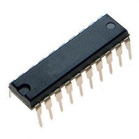
ETC5067N/C STMicroelectronics, ETC5067N/C Datasheet - Page 8

ETC5067N/C
Manufacturer Part Number
ETC5067N/C
Description
Telecom ICs Interfc CODEC Filter
Manufacturer
STMicroelectronics
Type
Telecom ICs - Variousr
Datasheet
1.ETC5064DC013TR.pdf
(18 pages)
Specifications of ETC5067N/C
Operating Supply Voltage
7 V
Operating Temperature Range
- 25 C to + 125 C
Mounting Style
Through Hole
Operating Frequency
2.048 MHz
Package / Case
PDIP-20
Lead Free Status / RoHS Status
Lead free / RoHS Compliant
Available stocks
Company
Part Number
Manufacturer
Quantity
Price
Part Number:
ETC5067N/C
Manufacturer:
ST
Quantity:
20 000
ETC5064 - ETC5064-X - ETC5067 - ETC5067-X
All TIMING SPECIFICATIONS
Note : 1.For short frame sync timing. FS
Figure 1 : 64 k bits/s TIMING DIAGRAM. (see next page for complete timing)
8/18
Symbol
t
t
1/t
t
t
t
t
t
SBFM
t
t
t
t
t
t
t
HOLD
t
t
WMH
WML
t
t
WBH
HBFI
t
WBL
t
t
DBD
DZC
SDB
HBD
t
t
XDP
WFL
HBF
SFB
DZF
RM
FM
RB
PB
FB
SF
HF
PM
Frequency of master clocks
MCLK
Depends on the device used and the
BCLK
Width of Master Clock High
Width of Master Clock Low
Rise Time of Master Clock
Fall Time of Master Clock
Period of Bit Clock
Width of Bit Clock High (V
Width of Bit Clock Low (V
Rise Time of Bit Clock (t
Fall Time of Bit Clock (t
Set-up time from BCLK
(first bit clock after the leading edge of FS
Holding Time from Bit Clock Low to the Frame Sync
(long frame only)
Set-up Time from Frame Sync to Bit Clock (long frame only)
Hold Time from 3rd Period of Bit Clock
Low to Frame Sync (long frame only)
Delay Time to valid data from FS
comes later and delay time from FSX to data output disabled
(C
Delay Time from BCLK
(load = 150 pF plus 2 LSTTL loads)
Delay Time from BCLK
Set-up Time from D
Hold Time from BCLK
Holding Time from Bit Clock High to Frame Sync (short frame only)
Set-up Time from FS
(short frame sync pulse) - Note 1
Hold Time from BCLK
(short frame sync pulse) - Note 1
Delay Time to TS
Minimum Width of the Frame Sync Pulse (low level)
(64 bit/s operating mode)
L
= 0 pF to 150 pF)
R
X
/CLKSEL Pin
and MCLK
X
R
low (load = 150 pF plus 2 LSTTI loads)
R
X/R
valid to BCLK
R/X
X/R
X
X
X
X
PB
and FS
PB
to BCLK
high to data valid
low to data output disabled
high to MCLK
low to D
Low to FS
IL
IH
= 488 ns)
Parameter
= 488 ns)
= 0.6 V)
= 2.2 V)
R
X/R
must go high while their respective bit clocks are high.
X
R
or BCLK
R/X
invalid
X/R
Low
X
low
Low
falling edge.
X
)
X
MCLK
MCLK
MCLK
MCLK
, whichever
X
X
X
X
and MCLK
and MCLK
and MCLK
and MCLK
FS
X
or FS
R
R
R
R
R
Min.
485
160
160
160
160
100
100
100
160
80
20
50
50
50
80
0
0
0
1.536
2.048
1.544
Typ.
488
15.725
Max.
165
150
165
140
50
50
50
50
MHz
Unit
ns
ns
ns
ns
ns
ns
ns
ns
ns
ns
ns
ns
ns
ns
ns
ns
ns
ns
ns
ns
ns
ns
ns


