IPB034N03L G Infineon Technologies, IPB034N03L G Datasheet - Page 2
IPB034N03L G
Manufacturer Part Number
IPB034N03L G
Description
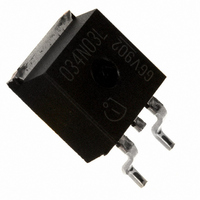
MOSFET N-CH 30V 80A TO-263-3
Manufacturer
Infineon Technologies
Series
OptiMOS™r
Datasheet
1.IPP034N03L_G.pdf
(10 pages)
Specifications of IPB034N03L G
Package / Case
D²Pak, TO-263 (2 leads + tab)
Fet Type
MOSFET N-Channel, Metal Oxide
Fet Feature
Logic Level Gate
Rds On (max) @ Id, Vgs
3.4 mOhm @ 30A, 10V
Drain To Source Voltage (vdss)
30V
Current - Continuous Drain (id) @ 25° C
80A
Vgs(th) (max) @ Id
2.2V @ 250µA
Gate Charge (qg) @ Vgs
51nC @ 10V
Input Capacitance (ciss) @ Vds
5300pF @ 15V
Power - Max
94W
Mounting Type
Surface Mount
Minimum Operating Temperature
- 55 C
Configuration
Single
Transistor Polarity
N-Channel
Resistance Drain-source Rds (on)
0.0034 Ohm @ 10 V
Drain-source Breakdown Voltage
30 V
Gate-source Breakdown Voltage
+/- 20 V
Continuous Drain Current
80 A
Power Dissipation
94000 mW
Maximum Operating Temperature
+ 175 C
Mounting Style
SMD/SMT
Drain Source Voltage Vds
30V
On Resistance Rds(on)
2.8mohm
Rds(on) Test Voltage Vgs
10V
Operating Temperature Range
-55°C To +175°C
Transistor Case Style
TO-263
Rohs Compliant
Yes
Lead Free Status / RoHS Status
Lead free / RoHS Compliant
Lead Free Status / RoHS Status
Lead free / RoHS Compliant, Lead free / RoHS Compliant
Other names
IPB034N03LGINTR
IPB034N03LGXT
SP000304126
IPB034N03LGXT
SP000304126


Rev. 2.0
2)
3)
4)
connection. PCB is vertical in still air.
5)
Maximum ratings, at T
Parameter
Power dissipation
Operating and storage temperature
IEC climatic category; DIN IEC 68-1
Parameter
Thermal characteristics
Thermal resistance, junction - case
SMD version, device on PCB
Electrical characteristics, at T
Static characteristics
Drain-source breakdown voltage
Gate threshold voltage
Zero gate voltage drain current
Gate-source leakage current
Drain-source on-state resistance
Gate resistance
Transconductance
See figure 3 for more detailed information
See figure 13 for more detailed information
Device on 40 mm x 40 mm x 1.5 mm epoxy PCB FR4 with 6 cm2 (one layer, 70 µm thick) copper area for drain
Measured from drain tab to source pin
j
=25 ° C, unless otherwise specified
j
=25 ° C, unless otherwise specified
5)
Symbol Conditions
P
T
Symbol Conditions
R
R
V
V
I
I
R
R
g
DSS
GSS
fs
j
tot
(BR)DSS
GS(th)
thJC
thJA
DS(on)
G
, T
stg
T
minimal footprint
6 cm² cooling area
V
V
V
T
V
T
V
V
V
|V
I
D
page 2
C
j
j
GS
DS
DS
DS
GS
GS
GS
=25 ° C
=125 ° C
=30 A
DS
=25 °C
=0 V, I
=V
=30 V, V
=30 V, V
=20 V, V
=4.5 V, I
=10 V, I
|>2|I
GS
, I
D
|R
D
D
=1 mA
D
=250 µA
D
GS
GS
DS(on)max
DS
=30 A
=30 A
=0 V,
=0 V,
=0 V
4)
,
min.
30
50
1
-
-
-
-
-
-
-
-
-
-55 ... 175
55/175/56
Values
Value
typ.
100
0.1
3.8
2.8
1.6
94
10
10
-
-
-
-
-
IPB034N03L G
IPP034N03L G
max.
100
100
1.6
2.2
4.7
3.4
62
40
1
-
-
-
Unit
W
° C
Unit
K/W
V
µA
nA
mW
W
S
2010-02-19
Related parts for IPB034N03L G
Image
Part Number
Description
Manufacturer
Datasheet
Request
R

Part Number:
Description:
Manufacturer:
Infineon Technologies AG
Datasheet:
Part Number:
Description:
Manufacturer:
Infineon Technologies AG
Datasheet:
Part Number:
Description:
Manufacturer:
Infineon Technologies AG
Datasheet:
Part Number:
Description:
Manufacturer:
Infineon Technologies AG
Datasheet:
Part Number:
Description:
Manufacturer:
Infineon Technologies AG
Datasheet:
Part Number:
Description:
Manufacturer:
Infineon Technologies AG
Datasheet:
Part Number:
Description:
Manufacturer:
Infineon Technologies AG
Datasheet:
Part Number:
Description:
16-bit microcontroller with 2x2 KByte RAM
Manufacturer:
Infineon Technologies AG
Datasheet:
Part Number:
Description:
NPN silicon RF transistor
Manufacturer:
Infineon Technologies AG
Datasheet:
Part Number:
Description:
NPN silicon RF transistor
Manufacturer:
Infineon Technologies AG
Datasheet:
Part Number:
Description:
NPN silicon RF transistor
Manufacturer:
Infineon Technologies AG
Datasheet:
Part Number:
Description:
NPN silicon RF transistor
Manufacturer:
Infineon Technologies AG
Datasheet:
Part Number:
Description:
Si-MMIC-amplifier in SIEGET 25-technologie
Manufacturer:
Infineon Technologies AG
Datasheet:
Part Number:
Description:
IGBT Power Module
Manufacturer:
Infineon Technologies AG
Datasheet:
Part Number:
Description:
IC for switching-mode power supplies
Manufacturer:
Infineon Technologies AG
Datasheet: