BUK9618-55A,118 NXP Semiconductors, BUK9618-55A,118 Datasheet - Page 5
BUK9618-55A,118
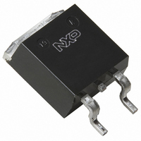
Manufacturer Part Number
BUK9618-55A,118
Description
MOSFET N-CH 55V 61A SOT404
Manufacturer
NXP Semiconductors
Series
TrenchMOS™r
Specifications of BUK9618-55A,118
Package / Case
D²Pak, TO-263 (2 leads + tab)
Fet Type
MOSFET N-Channel, Metal Oxide
Fet Feature
Logic Level Gate
Rds On (max) @ Id, Vgs
16 mOhm @ 25A, 10V
Drain To Source Voltage (vdss)
55V
Current - Continuous Drain (id) @ 25° C
61A
Vgs(th) (max) @ Id
2V @ 1mA
Gate Charge (qg) @ Vgs
34nC @ 5V
Input Capacitance (ciss) @ Vds
2210pF @ 25V
Power - Max
136W
Mounting Type
Surface Mount
Minimum Operating Temperature
- 55 C
Configuration
Single
Transistor Polarity
N-Channel
Resistance Drain-source Rds (on)
0.016 Ohm @ 10 V
Drain-source Breakdown Voltage
55 V
Gate-source Breakdown Voltage
+/- 15 V
Continuous Drain Current
61 A
Power Dissipation
136000 mW
Maximum Operating Temperature
+ 175 C
Mounting Style
SMD/SMT
Lead Free Status / RoHS Status
Lead free / RoHS Compliant
Lead Free Status / RoHS Status
Lead free / RoHS Compliant, Lead free / RoHS Compliant
Other names
934056812118
BUK9618-55A /T3
BUK9618-55A /T3
BUK9618-55A /T3
BUK9618-55A /T3


Philips Semiconductors
8. Characteristics
Table 5:
T
9397 750 08461
Product data
Symbol
Static characteristics
V
V
I
I
R
Dynamic characteristics
Q
Q
Q
C
C
C
t
t
t
t
L
L
DSS
GSS
d(on)
r
d(off)
f
j
d
s
(BR)DSS
GS(th)
DSon
iss
oss
rss
g(tot)
gs
gd
= 25 C unless otherwise specified
Characteristics
Parameter
drain-source breakdown
voltage
gate-source threshold voltage I
drain-source leakage current
gate-source leakage current
drain-source on-state
resistance
total gate charge
gate-to-source charge
gate-to-drain (Miller) charge
input capacitance
output capacitance
reverse transfer capacitance
turn-on delay time
rise time
turn-off delay time
fall time
internal drain inductance
internal source inductance
Conditions
I
V
V
V
Figure 7
V
V
V
I
V
f = 1 MHz;
V
V
from drain lead 6 mm from
package to centre of die
from contact screw on
mounting base to centre of die
SOT78
from upper edge of drain
mounting base to centre of die
SOT404
from source lead to source
bond pad
D
D
D
DS
GS
GS
GS
GS
GS
GS
DD
GS
T
T
T
T
T
T
T
T
T
= 0.25 mA; V
= 1 mA; V
= 25 A;
j
j
j
j
j
j
j
j
j
= 55 V; V
= 25 C
= 55 C
= 25 C
= 175 C
= 55 C
= 25 C
= 175 C
= 10 V; V
= 5 V; I
= 25 C
= 175 C
= 4.5 V; I
= 10 V; I
= 5 V; V
= 0 V; V
= 30 V; R
= 5 V; R
Rev. 01 — 27 August 2001
and
Figure 14
Figure 12
BUK9518-55A; BUK9618-55A
D
DS
DD
DS
G
D
8
= 25 A;
D
GS
L
= 10
= 25 A
DS
= V
= 25 A
GS
= 44 V;
= 25 V;
= 1.2 ;
= 0 V
= 0 V
= 0 V
GS
;
Figure 9
Min
55
50
1
0.5
TrenchMOS™ logic level FET
© Koninklijke Philips Electronics N.V. 2001. All rights reserved.
Typ
1.5
0.05
2
14
12
34
4.5
14
1660
290
190
21
126
95
97
4.5
3.5
2.5
7.5
Max
2
2.3
10
500
100
18
36
19
16
2210
350
270
5 of 14
Unit
V
V
V
V
V
nA
m
m
m
m
nC
nC
nC
pF
pF
pF
ns
ns
ns
ns
nH
nH
nH
nH
A
A
Related parts for BUK9618-55A,118
Image
Part Number
Description
Manufacturer
Datasheet
Request
R

Part Number:
Description:
Logic level N-channel enhancement mode Field-Effect Transistor (FET) in a plastic package using TrenchMOS technology
Manufacturer:
NXP Semiconductors
Datasheet:

Part Number:
Description:
MOSFET Power TAPE13 MOSFET
Manufacturer:
NXP Semiconductors

Part Number:
Description:
NXP Semiconductors designed the LPC2420/2460 microcontroller around a 16-bit/32-bitARM7TDMI-S CPU core with real-time debug interfaces that include both JTAG andembedded trace
Manufacturer:
NXP Semiconductors
Datasheet:

Part Number:
Description:
NXP Semiconductors designed the LPC2458 microcontroller around a 16-bit/32-bitARM7TDMI-S CPU core with real-time debug interfaces that include both JTAG andembedded trace
Manufacturer:
NXP Semiconductors
Datasheet:
Part Number:
Description:
NXP Semiconductors designed the LPC2468 microcontroller around a 16-bit/32-bitARM7TDMI-S CPU core with real-time debug interfaces that include both JTAG andembedded trace
Manufacturer:
NXP Semiconductors
Datasheet:
Part Number:
Description:
NXP Semiconductors designed the LPC2470 microcontroller, powered by theARM7TDMI-S core, to be a highly integrated microcontroller for a wide range ofapplications that require advanced communications and high quality graphic displays
Manufacturer:
NXP Semiconductors
Datasheet:
Part Number:
Description:
NXP Semiconductors designed the LPC2478 microcontroller, powered by theARM7TDMI-S core, to be a highly integrated microcontroller for a wide range ofapplications that require advanced communications and high quality graphic displays
Manufacturer:
NXP Semiconductors
Datasheet:
Part Number:
Description:
The Philips Semiconductors XA (eXtended Architecture) family of 16-bit single-chip microcontrollers is powerful enough to easily handle the requirements of high performance embedded applications, yet inexpensive enough to compete in the market for hi
Manufacturer:
NXP Semiconductors
Datasheet:
Part Number:
Description:
The XA-S3 device is a member of Philips Semiconductors? XA(eXtended Architecture) family of high performance 16-bitsingle-chip microcontrollers
Manufacturer:
NXP Semiconductors
Datasheet:

Part Number:
Description:
The NXP BlueStreak LH75401/LH75411 family consists of two low-cost 16/32-bit System-on-Chip (SoC) devices
Manufacturer:
NXP Semiconductors
Datasheet:
Part Number:
Description:
The NXP LPC3130/3131 combine an 180 MHz ARM926EJ-S CPU core, high-speed USB2
Manufacturer:
NXP Semiconductors
Datasheet:
Part Number:
Description:
The NXP LPC3141 combine a 270 MHz ARM926EJ-S CPU core, High-speed USB 2
Manufacturer:
NXP Semiconductors
Part Number:
Description:
The NXP LPC3143 combine a 270 MHz ARM926EJ-S CPU core, High-speed USB 2
Manufacturer:
NXP Semiconductors

Part Number:
Description:
The NXP LPC3152 combines an 180 MHz ARM926EJ-S CPU core, High-speed USB 2
Manufacturer:
NXP Semiconductors