PSMN005-55B,118 NXP Semiconductors, PSMN005-55B,118 Datasheet - Page 3
PSMN005-55B,118
Manufacturer Part Number
PSMN005-55B,118
Description
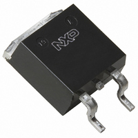
MOSFET N-CH 55V 75A SOT404
Manufacturer
NXP Semiconductors
Series
TrenchMOS™r
Datasheet
1.PSMN005-55B118.pdf
(12 pages)
Specifications of PSMN005-55B,118
Fet Type
MOSFET N-Channel, Metal Oxide
Fet Feature
Logic Level Gate
Rds On (max) @ Id, Vgs
5.8 mOhm @ 25A, 10V
Drain To Source Voltage (vdss)
55V
Current - Continuous Drain (id) @ 25° C
75A
Vgs(th) (max) @ Id
2V @ 1mA
Gate Charge (qg) @ Vgs
103nC @ 5V
Input Capacitance (ciss) @ Vds
6500pF @ 25V
Power - Max
230W
Mounting Type
Surface Mount
Package / Case
D²Pak, TO-263 (2 leads + tab)
Lead Free Status / RoHS Status
Lead free / RoHS Compliant
Other names
934055637118
PSMN005-55B /T3
PSMN005-55B /T3
PSMN005-55B /T3
PSMN005-55B /T3


Philips Semiconductors
October 1999
THERMAL RESISTANCES
AVALANCHE ENERGY LIMITING VALUES
Limiting values in accordance with the Absolute Maximum System (IEC 134)
ELECTRICAL CHARACTERISTICS
T
SYMBOL PARAMETER
R
R
SYMBOL PARAMETER
E
I
SYMBOL PARAMETER
V
V
R
I
I
Q
Q
Q
t
t
t
t
L
L
L
C
C
C
j
= 25˚C unless otherwise specified
N-channel logic level TrenchMOS
AS
GSS
DSS
d on
r
d off
f
d
d
s
AS
(BR)DSS
GS(TO)
th j-mb
th j-a
DS(ON)
iss
oss
rss
g(tot)
gs
gd
Thermal resistance junction
to mounting base
Thermal resistance junction
to ambient
Non-repetitive avalanche
energy
Non-repetitive avalanche
current
Drain-source breakdown
voltage
Gate threshold voltage
Drain-source on-state
resistance
Gate source leakage current V
Zero gate voltage drain
current
Total gate charge
Gate-source charge
Gate-drain (Miller) charge
Turn-on delay time
Turn-on rise time
Turn-off delay time
Turn-off fall time
Internal drain inductance
Internal drain inductance
Internal source inductance
Input capacitance
Output capacitance
Feedback capacitance
CONDITIONS
SOT78 package, in free air
SOT404 package, pcb mounted, minimum
footprint
CONDITIONS
Unclamped inductive load, I
t
V
CONDITIONS
V
V
V
V
V
V
V
I
V
V
Resistive load
Measured from tab to centre of die
Measured from drain lead to centre of die
(SOT78 package only)
Measured from source lead to source
bond pad
V
p
D
DD
GS
DS
GS
GS
GS
GS
GS
DS
DD
GS
GS
= 75 A; V
= 100 s; T
= 0 V; I
= V
= 10 V; I
= 5 V; I
= 4.5 V; I
= 5 V; I
=
= 55 V; V
= 30 V; R
= 5 V; R
= 0 V; V
15 V; R
GS
10 V; V
(TM)
; I
D
D
D
D
DD
DS
G
D
= 0.25 mA;
= 1 mA
= 25 A
= 25 A; T
D
GS
j
GS
D
= 44 V; V
= 10
= 25 A
prior to avalanche = 25˚C;
3
transistor
= 25 V; f = 1 MHz
= 25 A
= 1.2 ;
DS
= 0 V;
= 50 ; V
= 0 V
j
GS
= 175˚C
GS
= 5 V
AS
= 5 V
= 75 A;
T
T
T
T
j
j
j
j
= 175˚C
= 175˚C
= -55˚C
= -55˚C
MIN. TYP. MAX. UNIT
1.0
0.5
TYP.
55
50
MIN.
-
-
-
-
-
-
-
-
-
-
-
-
-
-
-
-
-
-
-
-
-
60
50
PSMN005-55B;
-
-
-
PSMN005-55P
6500
1500
0.05
103
180
420
235
700
1.5
4.8
5.3
3.5
4.5
7.5
Product specification
15
52
45
2
-
-
-
-
-
-
-
MAX.
MAX.
0.65
268
75
-
-
13.2
100
500
2.0
2.3
5.8
6.3
6.7
10
-
-
-
-
-
-
-
-
-
-
-
-
-
-
-
-
Rev 1.200
UNIT
UNIT
K/W
K/W
K/W
mJ
A
m
m
m
m
nA
nC
nC
nC
nH
nH
nH
pF
pF
pF
ns
ns
ns
ns
V
V
V
V
V
A
A
Related parts for PSMN005-55B,118
Image
Part Number
Description
Manufacturer
Datasheet
Request
R

Part Number:
Description:
MOSFET N-CH 75V 75A D2PAK
Manufacturer:
NXP Semiconductors
Datasheet:

Part Number:
Description:
MOSFET N-CH 75V 75A TO220AB
Manufacturer:
NXP Semiconductors
Datasheet:

Part Number:
Description:
SiliconMAX standard level N-channel enhancement mode Field-Effect Transistor (FET) in a plastic package using TrenchMOS technology
Manufacturer:
NXP Semiconductors
Datasheet:

Part Number:
Description:
MOSFET N-CH 30V 20A SOT96-1
Manufacturer:
NXP Semiconductors
Datasheet:

Part Number:
Description:
SiliconMAX logic level N-channel enhancement mode Field-Effect Transistor (FET) in a plastic package using TrenchMOS technology
Manufacturer:
NXP Semiconductors
Datasheet:

Part Number:
Description:
N-channel Logic Level Field-effect Power Transistor In A Plastic Package Using Trenchmos Technology.
Manufacturer:
NXP Semiconductors
Datasheet:
Part Number:
Description:
Psmn005-25d N-channel Logic Level Trenchmos Tm Transistor
Manufacturer:
NXP Semiconductors
Datasheet:
Part Number:
Description:
Psmn005-30k Trenchmos Tm Logic Level Fet
Manufacturer:
NXP Semiconductors
Datasheet:

Part Number:
Description:
MOSFET N-CH 25V 75A SOT428
Manufacturer:
NXP Semiconductors
Datasheet:
Part Number:
Description:
MOSFET N-CH 55V 75A SOT78
Manufacturer:
NXP Semiconductors
Datasheet:
Part Number:
Description:
MOSFET TAPE13 PWR-MOS
Manufacturer:
NXP Semiconductors
Datasheet:

Part Number:
Description:
N-channel logic level TrenchMOS transistor
Manufacturer:
PHILIPS [NXP Semiconductors]
Datasheet:
Part Number:
Description:
NXP Semiconductors designed the LPC2420/2460 microcontroller around a 16-bit/32-bitARM7TDMI-S CPU core with real-time debug interfaces that include both JTAG andembedded trace
Manufacturer:
NXP Semiconductors
Datasheet: