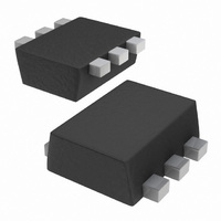
PEMD9,115 NXP Semiconductors, PEMD9,115 Datasheet

PEMD9,115
Specifications of PEMD9,115
PEMD9 T/R
PEMD9 T/R
Available stocks
Related parts for PEMD9,115
PEMD9,115 Summary of contents
Page 1
DATA SHEET PEMD9; PUMD9 NPN/PNP resistor-equipped transistors kΩ kΩ Product data sheet Supersedes data of 2003 Nov 04 DISCRETE SEMICONDUCTORS 2004 Apr 15 ...
Page 2
... NXP Semiconductors NPN/PNP resistor-equipped transistors kΩ kΩ FEATURES • Built-in bias resistors • Simplifies circuit design • Reduces component count • Reduces pick and place costs. APPLICATIONS • Low current peripheral driver • Replacement of general purpose transistors in digital applications • Control of IC inputs. ...
Page 3
... NXP Semiconductors NPN/PNP resistor-equipped transistors kΩ kΩ ORDERING INFORMATION TYPE NUMBER NAME − PEMD9 − PUMD9 LIMITING VALUES In accordance with the Absolute Maximum Rating System (IEC 60134). SYMBOL PARAMETER Per transistor; for the PNP transistor with negative polarity V collector-base voltage CBO ...
Page 4
... NXP Semiconductors NPN/PNP resistor-equipped transistors kΩ kΩ THERMAL CHARACTERISTICS SYMBOL PARAMETER Per transistor R thermal resistance from junction to th(j-a) ambient SOT363 SOT666 Per device R thermal resistance from junction to th(j-a) ambient SOT363 SOT666 Notes 1. Transistor mounted on an FR4 printed-circuit board, single-sided copper, standard footprint. ...
Page 5
... NXP Semiconductors NPN/PNP resistor-equipped transistors kΩ kΩ CHARACTERISTICS = 25 °C; unless otherwise specified. T amb SYMBOL PARAMETER Per transistor; for the PNP transistor with negative polarity I collector-base cut-off current CBO I collector-emitter cut-off current CEO I emitter-base cut-off current EBO h DC current gain FE V collector-emitter saturation voltage ...
Page 6
... NXP Semiconductors NPN/PNP resistor-equipped transistors kΩ kΩ PACKAGE OUTLINES Plastic surface-mounted package; 6 leads pin 1 index DIMENSIONS (mm are the original dimensions) UNIT 0.6 0.27 0.18 1.7 mm 0.5 0.17 0.08 1.5 OUTLINE VERSION IEC SOT666 2004 Apr scale 1.3 1.7 0.3 1.0 0.5 1 ...
Page 7
... NXP Semiconductors NPN/PNP resistor-equipped transistors kΩ kΩ Plastic surface-mounted package; 6 leads y 6 pin 1 index DIMENSIONS (mm are the original dimensions UNIT max 0.30 1.1 0.25 mm 0.1 0.20 0.8 0.10 OUTLINE VERSION IEC SOT363 2004 Apr scale 2.2 1.35 2.2 1.3 0.65 1.8 1 ...
Page 8
... NXP Semiconductors. In case of any inconsistency or conflict between information in this document and such terms and conditions, the latter will prevail. ...
Page 9
... NXP Semiconductors Customer notification This data sheet was changed to reflect the new company name NXP Semiconductors, including new legal definitions and disclaimers. No changes were made to the technical content, except for package outline drawings which were updated to the latest version. Contact information For additional information please visit: http://www ...


