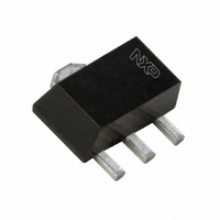
2PB1424,115 NXP Semiconductors, 2PB1424,115 Datasheet - Page 10

2PB1424,115
Manufacturer Part Number
2PB1424,115
Description
TRANSISTOR PNP 20V 3.0A SC-62
Manufacturer
NXP Semiconductors
Series
-r
Datasheet
1.2PB1424115.pdf
(13 pages)
Specifications of 2PB1424,115
Package / Case
SC-62, SOT-89, TO-243 (3 Leads + Tab)
Transistor Type
PNP
Current - Collector (ic) (max)
3A
Voltage - Collector Emitter Breakdown (max)
20V
Vce Saturation (max) @ Ib, Ic
500mV @ 100mA, 2A
Dc Current Gain (hfe) (min) @ Ic, Vce
180 @ 100mA, 2V
Power - Max
2W
Frequency - Transition
125MHz
Mounting Type
Surface Mount
Dc Collector/base Gain Hfe Min
180
Gain Bandwidth Product Ft
125 MHz
Minimum Operating Temperature
- 65 C
Configuration
Single
Transistor Polarity
PNP
Mounting Style
SMD/SMT
Collector- Emitter Voltage Vceo Max
- 20 V
Emitter- Base Voltage Vebo
- 6 V
Continuous Collector Current
- 3 A
Maximum Dc Collector Current
- 5 A
Power Dissipation
2 W
Maximum Operating Frequency
125 MHz
Maximum Operating Temperature
+ 150 C
Current - Collector Cutoff (max)
-
Lead Free Status / RoHS Status
Lead free / RoHS Compliant
Current - Collector Cutoff (max)
-
Lead Free Status / Rohs Status
Lead free / RoHS Compliant
Other names
934059291115
NXP Semiconductors
10. Soldering
2PB1424_2
Product data sheet
Fig 15. Reflow soldering footprint SOT89 (SC-62/TO-243)
Fig 16. Wave soldering footprint SOT89 (SC-62/TO-243)
4.60
0.85
SOT89 standard mounting conditions for reflow soldering
Not recommended for wave soldering
1.20
1.20
1.00
(3x)
0.20
1.50
3
6.60
2.40
0.70
5.30
Rev. 02 — 15 January 2007
3
1.20
3.70
3.95
4.75
2.25
2.00
1.90
2
1
2
0.50
1.20
20 V, 3 A PNP low V
3.50
3.00
1
0.60 (3x)
0.70 (3x)
7.60
0.50
preferred transport direction during soldering
1.20
1.70
4.85
Dimensions in mm
msa442
CEsat
solder lands
solder resist
occupied area
Dimensions in mm
2PB1424
© NXP B.V. 2007. All rights reserved.
(BISS) transistor
solder lands
solder resist
occupied area
solder paste
msa423
10 of 13


