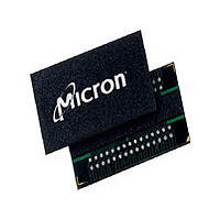
MT46V16M16CY-6 IT:K Micron Technology Inc, MT46V16M16CY-6 IT:K Datasheet - Page 85

MT46V16M16CY-6 IT:K
Manufacturer Part Number
MT46V16M16CY-6 IT:K
Description
DRAM Chip DDR SDRAM 256M-Bit 16Mx16 2.5V 60-Pin FBGA Tray
Manufacturer
Micron Technology Inc
Type
DDR SDRAMr
Datasheet
1.MT46V16M16CY-6_ITK.pdf
(93 pages)
Specifications of MT46V16M16CY-6 IT:K
Density
256 Mb
Maximum Clock Rate
333 MHz
Package
60FBGA
Address Bus Width
15 Bit
Operating Supply Voltage
2.5 V
Maximum Random Access Time
0.7 ns
Operating Temperature
-40 to 85 °C
Organization
16Mx16
Address Bus
15b
Access Time (max)
700ps
Operating Supply Voltage (typ)
2.5V
Package Type
FBGA
Operating Temp Range
-40C to 85C
Operating Supply Voltage (max)
2.7V
Operating Supply Voltage (min)
2.3V
Supply Current
270mA
Pin Count
60
Mounting
Surface Mount
Operating Temperature Classification
Industrial
Lead Free Status / RoHS Status
Compliant
Figure 48:
PDF: 09005aef80768abb/Source: 09005aef82a95a3a
DDR_x4x8x16_Core2.fm - 256Mb DDR: Rev. O, Core DDR: Rev. B 1/09 EN
Command
BA0, BA1
Address
DQS
DQ 5
CK#
CKE
A10
DM
CK
t
t
IS
IS
NOP 1
Bank WRITE – Without Auto Precharge
T0
t
t
IH
IH
Notes:
t
t
Bank x
IS
IS
Row
Row
ACT
T1
1. NOP commands are shown for ease of illustration; other commands may be valid at these
2. BL = 4.
3. Disable auto precharge.
4. “Don’t Care” if A10 is HIGH at T8.
5. DI b = data-in from column b; subsequent elements are provided in the programmed order.
6. See Figure 50 on page 85 for detailed DQ timing.
t
t
IH
IH
t
times.
CK
t
t
RCD
RAS
NOP 1
T2
t
CH
t
CL
WRITE 2
t
Bank x
Col n
IS
3
T3
t
t
DQSS (NOM)
IH
t
WPRES
t DS
83
t
WPRE
NOP 1
T4
DI
b
t DH
Micron Technology, Inc., reserves the right to change products or specifications without notice.
T4n
t
DQSL
NOP 1
T5
t
DQSH
256Mb: x4, x8, x16 DDR SDRAM
T5n
t
WPST
NOP 1
T6
Transitioning Data
©2003 Micron Technology, Inc. All rights reserved.
t
NOP 1
WR
T7
Operations
One bank
All banks
Don’t Care
Bank x 4
T8
PRE
t
RP


