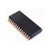
PCK2002MPW-T NXP Semiconductors, PCK2002MPW-T Datasheet - Page 2

PCK2002MPW-T
Manufacturer Part Number
PCK2002MPW-T
Description
Clock Buffer 14.318-167MHZ I2C 1:10CLK BUFR
Manufacturer
NXP Semiconductors
Datasheet
1.PCK2002MPW-T.pdf
(12 pages)
Specifications of PCK2002MPW-T
Number Of Outputs
10
Operating Supply Voltage (max)
3.465V
Operating Temp Range
0C to 70C
Propagation Delay Time
5ns
Operating Supply Voltage (min)
3.135V
Mounting
Surface Mount
Pin Count
28
Operating Supply Voltage (typ)
3.3V
Package Type
TSSOP
Quiescent Current
100uA
Input Frequency
133MHz
Duty Cycle
55%
Operating Temperature Classification
Commercial
Max Input Freq
133 MHz
Propagation Delay (max)
2.7 ns
Supply Voltage (max)
3.465 V
Supply Voltage (min)
3.135 V
Maximum Operating Temperature
+ 70 C
Minimum Operating Temperature
0 C
Mounting Style
SMD/SMT
Package / Case
TSSOP-28
Lead Free Status / RoHS Status
Compliant
Other names
PCK2002MPW,118
FEATURES
QUICK REFERENCE DATA
ORDERING INFORMATION
PIN CONFIGURATION
Intel and Pentium are registered trademarks of Intel Corporation.
I
2
Philips Semiconductors
2001 Jul 19
C is a trademark of Philips Semiconductors Corporation.
HIGH speed, LOW noise non-inverting 1:10 buffer
Mobile (reduced pincount) version of PCK2002
Typically used to support two SDRAM DIMMs
28-pin SSOP and TSSOP packages
See PCK2002 for 48-pin 1-18 buffer part supporting up to
4 SDRAM DIMMs
Optimized for 66 MHz, 100 MHz and 133 MHz operation
Multiple V
Spread spectrum compliant
175 ps skew outputs
Individual clock output enable/disable via I
0–300 MHz I
SYMBOL
28-Pin Plastic TSSOP
28-Pin Plastic SSOP
I
t
t
CC
PLH
PHL
t
t
r
f
PACKAGES
DD
BUF_OUT16
and V
BUF_OUT0
BUF_OUT2
BUF_OUT3
BUF_OUT1
Propagation delay
BUF_IN to BUF_OUT
Rise time
Fall time
Total supply current
BUF_IN
V
V
V
DDI2C
V
V
V
V
SDA
SS
DD1
SS0
DD4
DD0
SS1
SS4
pins for noise reduction
2
10
11
12
13
14
C 1:10 clock buffer
1
2
3
4
5
6
7
8
9
TOP VIEW
PARAMETER
TEMPERATURE RANGE
n
28
27
26
25
24
23
22
21
20
19
18
17
16
15
2
C
SA00550
V
BUF_OUT15
BUF_OUT14
V
V
BUF_OUT13
BUF_OUT12
V
OE
V
BUF_OUT17
V
V
SCL
0 to +70 C
0 to +70 C
DD9
SS9
DD8
SS8
DD5
SS5
SSI2C
V
V
V
V
CC
CC
CC
CC
= 3.3 V, CL = 30 pF
= 3.3 V, CL = 30 pF
= 3.3 V, CL = 30 pF
= 3.465 V
2
All clock outputs meet Intel’s drive, rise/fall time, accuracy, and skew
DESCRIPTION
The PCK2002M is a 1–10 fanout buffer used for 133/100 MHz CPU,
66/33 MHz PCI, 14.318 MHz REF, or 133/100/66 MHz SDRAM
clock distribution. 10 outputs are typically used to support up to
2 SDRAM DIMMs commonly found in laptop or mobile applications.
The PCK2002M has the same features and operating characteristics
of the PCK2002 and is available in the SSOP 28 pin package.
requirements. An I
enabled/disabled individually. An output disabled via the I
interface will be held in the LOW state. In addition, there is an OE
input which 3-states all outputs.
PIN DESCRIPTION
22, 23, 26,
NUMBER
19, 24, 28
17, 21, 25
2, 3, 6, 7
1, 5, 10,
4, 8, 12,
11, 18
PIN
27
20
14
15
13
16
9
CONDITIONS
ORDER CODE
PCK2002MPW
PCK2002MDB
Output
Output
Output
TYPE
Input
Input
Input
Input
Input
Input
Input
I/O
I/O
2
C interface is included to allow each output to be
V
V
DD (0, 1, 4, 5, 8, 9)
SS (0, 1, 4, 5, 8, 9)
BUF_OUT
BUF_OUT
BUF_OUT
SYMBOL
(12–15)
(16–17)
BUF_IN
V
V
(0–3)
SDA
SCL
DDI2C
DDI2C
OE
DRAWING NUMBER
TYPICAL
Buffered clock outputs
Buffered clock outputs
Buffered clock outputs
Buffered clock input
Active high output
enable
I
I
3.3 V power supply
Ground
3.3 V I
I
2
2
2
C serial data
C serial clock
C ground
PCK2002M
2.7
2.9
1.1
1.0
35
SOT341–1
SOT361–1
FUNCTION
2
C power supply
853-2268 26745
Product data
2
C
UNIT
ns
ns
ns
A


