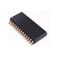
PCK2002MPW-T NXP Semiconductors, PCK2002MPW-T Datasheet - Page 9

PCK2002MPW-T
Manufacturer Part Number
PCK2002MPW-T
Description
Clock Buffer 14.318-167MHZ I2C 1:10CLK BUFR
Manufacturer
NXP Semiconductors
Datasheet
1.PCK2002MPW-T.pdf
(12 pages)
Specifications of PCK2002MPW-T
Number Of Outputs
10
Operating Supply Voltage (max)
3.465V
Operating Temp Range
0C to 70C
Propagation Delay Time
5ns
Operating Supply Voltage (min)
3.135V
Mounting
Surface Mount
Pin Count
28
Operating Supply Voltage (typ)
3.3V
Package Type
TSSOP
Quiescent Current
100uA
Input Frequency
133MHz
Duty Cycle
55%
Operating Temperature Classification
Commercial
Max Input Freq
133 MHz
Propagation Delay (max)
2.7 ns
Supply Voltage (max)
3.465 V
Supply Voltage (min)
3.135 V
Maximum Operating Temperature
+ 70 C
Minimum Operating Temperature
0 C
Mounting Style
SMD/SMT
Package / Case
TSSOP-28
Lead Free Status / RoHS Status
Compliant
Other names
PCK2002MPW,118
Philips Semiconductors
AC WAVEFORMS
V
V
V
V
output load.
TEST CIRCUIT
2001 Jul 19
M
X
Y
OL
0–300 MHz I
OUTPUT
LOW-to-OFF
OFF-to-LOW
OUTPUT
HIGH-to-OFF
OFF-to-HIGH
= V
= V
nOE INPUT
= 1.5 V
and V
BUF_OUT
GND
V
V
V
V
V
OL
OH
DD
SS
OL
OH
I
BUF_IN
INPUT
+ 0.3 V
–0.3 V
OH
Figure 1. Load circuitry for switching times.
Figure 2. 3-State enable and disable times
2.4
1.5
0.4
are the typical output voltage drop that occur with the
Figure 3. SDRAM Output clock
T
SDRISE
outputs
enabled
V
M
t
PLZ
t
PHZ
2
V
T
M
SDKH
t
C 1:10 clock buffer
PLH
T
SDFALL
V
T
X
SDKP
V
V
Y
M
V
DUTY CYCLE
M
T
outputs
disabled
SDKL
V
DD
t
PHL
V
t
M
PZL
t
SW00247
PZH
SW00246
V
M
V
SW00245
M
outputs
enabled
V
DD
9
GENERATOR
PULSE
Figure 4. Load circuitry for switching times
t
t
t
PLH
PHZ
V
PLZ
TEST
I
R
/t
/t
/t
T
PHL
PZL
PZH
D.U.T.
V
2 V
DD
Open
V
S
SS
1
DD
V
O
C
L
PCK2002M
S
SW00251
500
500
1
Product data
2 V
Open
V
SS
DD


