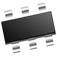
MCP4706A0T-E/CH Microchip Technology, MCP4706A0T-E/CH Datasheet - Page 11

MCP4706A0T-E/CH
Manufacturer Part Number
MCP4706A0T-E/CH
Description
Single, 8-bit NV DAC With Ext Vref And I2C Interface 6 SOT-23 T/R
Manufacturer
Microchip Technology
Series
-r
Datasheet
1.MCP4706A0T-ECH.pdf
(86 pages)
Specifications of MCP4706A0T-E/CH
Number Of Converters
1
Conversion Rate
1
Resolution
8 bit
Interface Type
I2C
Settling Time
6 us
Supply Voltage (max)
5.5 V
Supply Voltage (min)
2.7 V
Maximum Operating Temperature
+ 125 C
Mounting Style
SMD/SMT
Package / Case
SOT-23-6
Maximum Power Dissipation
452 mW
Minimum Operating Temperature
- 40 C
Supply Current
210 uA
Number Of Bits
8
Data Interface
EEPROM, I²C, Serial
Voltage Supply Source
Single Supply
Power Dissipation (max)
452mW
Operating Temperature
-40°C ~ 125°C
Mounting Type
Surface Mount
Number Of Outputs And Type
*
Lead Free Status / Rohs Status
Details
Available stocks
Company
Part Number
Manufacturer
Quantity
Price
Company:
Part Number:
MCP4706A0T-E/CH
Manufacturer:
MICROCHIP
Quantity:
15 000
TABLE 1-3:
© 2011 Microchip Technology Inc.
I
Note 1:
2
Param.
102A
102B
103A
103B
C AC Characteristics
No.
2:
3:
4:
5:
6:
7:
8:
(5)
(5)
(5)
(5)
As a transmitter, the device must provide this internal minimum delay time to bridge the undefined region
(minimum 300 ns) of the falling edge of SCL to avoid unintended generation of START or STOP conditions.
A fast-mode (400 kHz) I
requirement t
stretch the LOW period of the SCL signal. If such a device does stretch the LOW period of the SCL signal,
it must output the next data bit to the SDA line.
T
the SCL line is released.
The MCP47X6 device must provide a data hold time to bridge the undefined part between V
the falling edge of the SCL signal. This specification is not a part of the I
in order to ensure that the output data will meet the setup and hold specifications for the receiving device.
Use C
Not Tested. This parameter ensured by characterization.
A Master Transmitter must provide a delay to ensure that difference between SDA and SCL fall times do
not unintentionally create a Start or Stop condition.
If this parameter is too short, it can create an unintentional Start or Stop condition to other devices on the
I
affected.
Ensured by the T
The specification is not part of the I 2 C specification. T
2
R
C bus line. If this parameter is too long, the Data Input Setup (T
T
T
T
T
Sym
max.+t
RSCL
RSDA
FSDA
FSCL
b
I
2
in pF for the calculations.
C BUS DATA REQUIREMENTS (SLAVE MODE) (CONTINUED)
Data Input: This parameter must be longer than t
Data Output: This parameter is characterized, and tested indirectly by testing T
SU;DAT
Characteristic
SDA rise time
SCL rise time
SCL fall time
SDA fall time
SU;DAT
AA
= 1000 + 250 = 1250 ns (according to the standard-mode I
3.4 MHz specification test.
≥ 250 ns must then be met. This will automatically be the case if the device does not
2
C-bus device can be used in a standard-mode (100 kHz) I
Standard Operating Conditions (unless otherwise specified)
Operating Temperature
Operating Voltage V
1.7 MHz mode
1.7 MHz mode
3.4 MHz mode
3.4 MHz mode
1.7 MHz mode
3.4 MHz mode
1.7 MHz mode
3.4 MHz mode
1.7 MHz mode
3.4 MHz mode
100 kHz mode
400 kHz mode
100 kHz mode
400 kHz mode
100 kHz mode
400 kHz mode
100 kHz mode
400 kHz mode
20 + 0.1Cb
20 + 0.1Cb
20 + 0.1Cb
20 + 0.1Cb
DD
range is described in
Min
—
20
20
10
10
20
10
—
20
10
20
10
—
—
AA
MCP4706/4716/4726
= T
–40°C ≤ T
(4)
SP
HD:DAT
.
1000
1000
Max
300
160
300
160
300
300
300
300
160
80
40
80
80
80
40
80
SU:DAT
+ T
A
≤ +125°C (Extended)
FSDA
2
Units
) or Clock Low time (T
C specification, but must be tested
ns
ns
ns
ns
ns
ns
ns
ns
ns
ns
ns
ns
ns
ns
ns
ns
ns
ns
Electrical characteristics
2
(or T
C bus specification) before
C
10 to 400 pF (100 pF
maximum for 3.4 MHz
mode)
After a Repeated Start
condition or an
Acknowledge bit
After a Repeated Start
condition or an
Acknowledge bit
C
10 to 400 pF (100 pF max
for 3.4 MHz mode)
C
10 to 400 pF (100 pF max
for 3.4 MHz mode)
C
10 to 400 pF (100 pF max
for 3.4 MHz mode)
b
b
b
b
RSDA
is specified to be from
is specified to be from
is specified to be from
is specified to be from
2
C-bus system, but the
).
Conditions
DS22272A-page 11
AA
IH
parameter.
LOW
and V
) can be
IL
of


