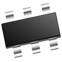
MCP4706A0T-E/CH Microchip Technology, MCP4706A0T-E/CH Datasheet - Page 59

MCP4706A0T-E/CH
Manufacturer Part Number
MCP4706A0T-E/CH
Description
Single, 8-bit NV DAC With Ext Vref And I2C Interface 6 SOT-23 T/R
Manufacturer
Microchip Technology
Series
-r
Datasheet
1.MCP4706A0T-ECH.pdf
(86 pages)
Specifications of MCP4706A0T-E/CH
Number Of Converters
1
Conversion Rate
1
Resolution
8 bit
Interface Type
I2C
Settling Time
6 us
Supply Voltage (max)
5.5 V
Supply Voltage (min)
2.7 V
Maximum Operating Temperature
+ 125 C
Mounting Style
SMD/SMT
Package / Case
SOT-23-6
Maximum Power Dissipation
452 mW
Minimum Operating Temperature
- 40 C
Supply Current
210 uA
Number Of Bits
8
Data Interface
EEPROM, I²C, Serial
Voltage Supply Source
Single Supply
Power Dissipation (max)
452mW
Operating Temperature
-40°C ~ 125°C
Mounting Type
Surface Mount
Number Of Outputs And Type
*
Lead Free Status / Rohs Status
Details
Available stocks
Company
Part Number
Manufacturer
Quantity
Price
Company:
Part Number:
MCP4706A0T-E/CH
Manufacturer:
MICROCHIP
Quantity:
15 000
7.0
7.1
The resolution is the number of DAC output states that
divide the full-scale range. For the 12-bit DAC, the
resolution is 2
to 4095.
7.2
Normally this is thought of as the ideal voltage
difference between two successive codes. This bit has
the smallest value or weight of all bits in the register.
For a given output voltage range, which is typically the
voltage between the Full-Scale voltage and the Zero-
Scale voltage (V
resolution of the device
EQUATION 7-1:
7.3
Normally this is thought of as the V
decreasing, as the DAC Register code is continuously
incremented by 1 code step (LSb).
7.4
The Full-scale error (see
offset error plus gain error. It is the difference between
the ideal and measured DAC output voltage with all bits
set to one (DAC input code = FFFh for 12-bit DAC).
EQUATION 7-2:
© 2011 Microchip Technology Inc.
Where:
2
N
FSE is expressed in LSb
V
V
V
= 4096 (MCP4726)
OUT(@FS)
IDEAL(@FS)
LSb
V
1024 (MCP4716)
256 (MCP4706)
FSE =
TERMINOLOGY
Resolution
Least Significant bit (LSb)
Monotonicity
Full-Scale Error (FSE)
LSb
is the delta voltage of one DAC register code
=
12
, meaning the DAC code ranges from 0
V
OUT(FS)
is the V
register code is at Full-scale.
DAC register code is at Full-scale.
step (such as code 000h to code 001h).
OUT(@FS)
is the ideal output voltage when the
V
OUT(FS)
LSb VOLTAGE
CALCULATION
FULL SCALE ERROR
OUT
(Equation
- V
V
2
- V
LSb
N
OUT(ZS)
Figure
voltage when the DAC
- V
- 1
IDEAL(@FS)
OUT(ZS)
7-1).
), it is divided by the
7-4) is the sum of
OUT
voltage never
7.5
The Zero-Scale Error (see
between the ideal and measured V
volatile DAC Register equal to 000h. The Zero-Scale
Error is the same as the Offset Error for this case
(volatile DAC Register = 000h).
EQUATION 7-3:
7.6
The Offset error (see
zero voltage output when the volatile DAC Register
value = 000h (zero scale voltage). This error affects all
codes by the same amount. The offset error can be
calibrated by software in application circuits.
FIGURE 7-1:
Offset
Error
(ZSE)
MCP4706/4716/4726
Where:
Analog
Output
FSE is expressed in LSb
V
V
OUT(@ZS)
LSb
ZSE =
Zero-Scale Error (ZSE)
Offset Error
0
is the delta voltage of one DAC register code
Actual Transfer Function
V
is the V
register code is at Zero-scale.
step (such as code 000h to code 001h).
OUT(@ZS)
V
LSb
Figure
ZERO SCALE ERROR
Offset Error Example.
OUT
Figure
voltage when the DAC
DAC Input Code
7-1) is the deviation from
Ideal Transfer Function
7-4) is the difference
OUT
DS22272A-page 59
voltage with the


