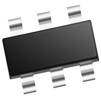
MCP4706A0T-E/CH Microchip Technology, MCP4706A0T-E/CH Datasheet - Page 64

MCP4706A0T-E/CH
Manufacturer Part Number
MCP4706A0T-E/CH
Description
Single, 8-bit NV DAC With Ext Vref And I2C Interface 6 SOT-23 T/R
Manufacturer
Microchip Technology
Series
-r
Datasheet
1.MCP4706A0T-ECH.pdf
(86 pages)
Specifications of MCP4706A0T-E/CH
Number Of Converters
1
Conversion Rate
1
Resolution
8 bit
Interface Type
I2C
Settling Time
6 us
Supply Voltage (max)
5.5 V
Supply Voltage (min)
2.7 V
Maximum Operating Temperature
+ 125 C
Mounting Style
SMD/SMT
Package / Case
SOT-23-6
Maximum Power Dissipation
452 mW
Minimum Operating Temperature
- 40 C
Supply Current
210 uA
Number Of Bits
8
Data Interface
EEPROM, I²C, Serial
Voltage Supply Source
Single Supply
Power Dissipation (max)
452mW
Operating Temperature
-40°C ~ 125°C
Mounting Type
Surface Mount
Number Of Outputs And Type
*
Lead Free Status / Rohs Status
Details
Available stocks
Company
Part Number
Manufacturer
Quantity
Price
Company:
Part Number:
MCP4706A0T-E/CH
Manufacturer:
MICROCHIP
Quantity:
15 000
MCP4706/4716/4726
8.2
The power source should be as clean as possible. The
power supply to the device is also used for the DAC
voltage reference internally if the internal V
selected as the resistor ladders reference voltage
(VREF1:VREF0 = 00 or 01).
Any noise induced on the V
performance. Typical applications will require a bypass
capacitor in order to filter out high frequency noise on
the V
supply’s traces or as a result of changes on the DAC
output. The bypass capacitor helps to minimize the
effect of these noise sources on signal integrity.
Figure 8-2
capacitors (a 10 µF tantalum capacitor and a 0.1 µF
ceramic capacitor) in parallel on the V
capacitors should be placed as close to the V
possible (within 4 mm). If the application circuit has
separate digital and analog power supplies, the V
and V
plane.
DS22272A-page 64
DD
SS
line. The noise can be induced onto the power
pins of the device should reside on the analog
Power Supply Considerations
shows an example of using two bypass
DD
line can affect the DAC
DD
line. These
DD
pin as
DD
DD
is
FIGURE 8-2:
with SOT-23 package.
Note: Pin assignment is opposite in DFN-6 package.
R1 and R2 are I
(Note: V
R1 and R2:
C1:
C2:
C3:
C4:
C5:
(a) Circuit when V
(b) Circuit when external reference is used.
5 kΩ - 10 kΩ for f
C1
C1
0.1 µF capacitor
10 µF capacitor
~ 0.1 µF
0.1 µF capacitor
10 µF capacitor
DD
V
C2
V
C2
V
V
~700Ω for f
OUT
V
OUT
V
SS
SS
DD
is connected to the reference circuit internally.)
DD
1
2
3
1
2
3
2
Optional
Optional
C pull-up resistors:
C3
C3
SCL
SCL
Analog
Output
Analog
Output
DD
Example MCP47X6 Circuit
© 2011 Microchip Technology Inc.
is selected as reference
=
=
6
5
4
6
5
4
Optional
100 kHz to 400 kHz
3.4 MHz
Ceramic
Tantalum
Optional to reduce noise
in V
Ceramic
Tantalum
V
SDA
SCL
V
SDA
SCL
C4
REF
REF
OUT
C5
pin.
V
REF
To MCU
To MCU
R1 R2
R1 R2
V
V
DD
DD


