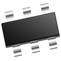
MCP4706A0T-E/CH Microchip Technology, MCP4706A0T-E/CH Datasheet - Page 34

MCP4706A0T-E/CH
Manufacturer Part Number
MCP4706A0T-E/CH
Description
Single, 8-bit NV DAC With Ext Vref And I2C Interface 6 SOT-23 T/R
Manufacturer
Microchip Technology
Series
-r
Datasheet
1.MCP4706A0T-ECH.pdf
(86 pages)
Specifications of MCP4706A0T-E/CH
Number Of Converters
1
Conversion Rate
1
Resolution
8 bit
Interface Type
I2C
Settling Time
6 us
Supply Voltage (max)
5.5 V
Supply Voltage (min)
2.7 V
Maximum Operating Temperature
+ 125 C
Mounting Style
SMD/SMT
Package / Case
SOT-23-6
Maximum Power Dissipation
452 mW
Minimum Operating Temperature
- 40 C
Supply Current
210 uA
Number Of Bits
8
Data Interface
EEPROM, I²C, Serial
Voltage Supply Source
Single Supply
Power Dissipation (max)
452mW
Operating Temperature
-40°C ~ 125°C
Mounting Type
Surface Mount
Number Of Outputs And Type
*
Lead Free Status / Rohs Status
Details
Available stocks
Company
Part Number
Manufacturer
Quantity
Price
Company:
Part Number:
MCP4706A0T-E/CH
Manufacturer:
MICROCHIP
Quantity:
15 000
MCP4706/4716/4726
3.1
V
has an output amplifier. V
approximately 0V to approximately V
range of the DAC output is from V
G is the gain selection option (1x or 2x).
In normal mode, the DC impedance of the output pin is
about 1Ω. In Power-Down mode, the output pin is
internally connected to a known pull-down resistor of
1 kΩ, 125 kΩ, or 640 kΩ. The Power-Down selection
bits settings are shown
3.2
V
supply voltage is relative to V
The power supply at the V
possible for a good DAC performance. It is
recommended to use an appropriate bypass capacitor
of about 0.1 µF (ceramic) to ground. An additional
10 µF
recommended to further attenuate high-frequency
noise present in application boards.
3.3
The V
The user must connect the V
through a low-impedance connection. If an analog
ground path is available in the application PCB (printed
circuit board), it is highly recommended that the V
be tied to the analog ground path or isolated within an
analog ground plane of the circuit board.
DS22272A-page 34
OUT
DD
is the positive supply voltage input pin. The input
SS
is the DAC analog output pin. The DAC output
capacitor
Analog Output Voltage Pin (V
Positive Power Supply Input (V
Ground (V
pin is the device ground reference.
(tantalum)
SS
Table
)
DD
pin should be as clean as
SS
4-2.
SS
OUT
.
in
pin to a ground plane
SS
can swing from
parallel
to G * V
DD
. The full-scale
RL
is
, where
OUT
SS
DD
also
pin
)
)
3.4
SDA is the serial data pin of the I
pin is used to write or read the DAC registers and
configuration bits. The SDA pin is an open-drain
N-channel driver. Therefore, it needs a pull-up resistor
from the V
stop conditions, the data on the SDA pin must be stable
during the high period of the clock. The high or low
state of the SDA pin can only change when the clock
signal on the SCL pin is low. Refer to
Serial Interface”
Interface communication.
3.5
SCL is the serial clock pin of the I
MCP47X6 devices act only as a slave and the SCL pin
accepts only external serial clocks. The input data from
the Master device is shifted into the SDA pin on the
rising edges of the SCL clock and output from the
device occurs at the falling edges of the SCL clock. The
SCL pin is an open-drain N-channel driver. Therefore,
it needs a pull-up resistor from the V
pin. Refer to
more details of I
3.6
This pin is used for the external voltage reference input.
The user can select V
voltage as the reference resistor ladder’s voltage
reference.
When the V
for this voltage to be buffered or unbuffered. This is
offered in cases where the reference voltage does not
have the current capability not to drop its voltage when
connected to the internal resistor ladder circuit.
When the V
is disconnected from the internal circuit.
See
Reference Voltage”
the configuration bits.
3.7
This pad is conductively connected to the device's
substrate. This pad should be tied to the same potential
as the V
used to assist as a heat sink for the device when
connected to a PCB heat sink.
Section 4.2
SS
Serial Clock Pin (SCL)
Voltage Reference Pin (V
Exposed Pad (EP)
Serial Data Pin (SDA)
DD
pin (or left unconnected). This pad could be
REF
DD
line to the SDA pin. Except for start and
Section 5.0 “I
is selected as reference voltage, this pin
pin signal is selected, there is an option
2
C Serial Interface communication.
for more details of I
and
“DAC’s
© 2011 Microchip Technology Inc.
DD
Table 4-4
voltage or the V
2
C Serial Interface”
2
(Resistor
C interface. The SDA
for more details on
2
DD
Section 5.0 “I
C interface. The
line to the SCL
REF
2
C Serial
)
Ladder)
REF
pin
2
for
C


