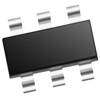
MCP4706A0T-E/CH Microchip Technology, MCP4706A0T-E/CH Datasheet - Page 39

MCP4706A0T-E/CH
Manufacturer Part Number
MCP4706A0T-E/CH
Description
Single, 8-bit NV DAC With Ext Vref And I2C Interface 6 SOT-23 T/R
Manufacturer
Microchip Technology
Series
-r
Datasheet
1.MCP4706A0T-ECH.pdf
(86 pages)
Specifications of MCP4706A0T-E/CH
Number Of Converters
1
Conversion Rate
1
Resolution
8 bit
Interface Type
I2C
Settling Time
6 us
Supply Voltage (max)
5.5 V
Supply Voltage (min)
2.7 V
Maximum Operating Temperature
+ 125 C
Mounting Style
SMD/SMT
Package / Case
SOT-23-6
Maximum Power Dissipation
452 mW
Minimum Operating Temperature
- 40 C
Supply Current
210 uA
Number Of Bits
8
Data Interface
EEPROM, I²C, Serial
Voltage Supply Source
Single Supply
Power Dissipation (max)
452mW
Operating Temperature
-40°C ~ 125°C
Mounting Type
Surface Mount
Number Of Outputs And Type
*
Lead Free Status / Rohs Status
Details
Available stocks
Company
Part Number
Manufacturer
Quantity
Price
Company:
Part Number:
MCP4706A0T-E/CH
Manufacturer:
MICROCHIP
Quantity:
15 000
4.5
To allow the application to conserve power when the
DAC operation is not required, three power down
modes are available. The Power-Down configuration
bits (PD1:PD0) control the power down operation
(Figure
• Turning off most of its internal circuits (op amp,
• Op amp output becomes high impedance to the
• Disconnects resistor ladder from reference
• Retains the value of the volatile DAC register and
Depending on the selected power down mode, the
following will occur:
• V
There is a delay (T
changing from ‘00’ to either ‘01’, ‘10’, or ‘11’ and the op
amp no longer driving the V
down resistors are sinking current.
In any of the power down modes, where the V
is not externally connected (sinking or sourcing
current), the power down current will typical be 60 nA
(see
Section 6.0 “MCP47X6 I2C Commands”
the I
commands that can update the volatile PD1:PD0 bits
are:
• Write Volatile DAC Register
• Write Volatile Memory
• Write All Memory
• Write Volatile Configuration bits
• General Call Reset
• General Call Wake-up
TABLE 4-2:
© 2011 Microchip Technology Inc.
resistor ladder, ...)
V
voltage (V
configuration bits, and the nonvolatile (EEPROM)
DAC register and configuration bits
downs (See
- 640kΩ (typical)
- 125kΩ (typical)
- 1kΩ (typical)
Note:
PD1
OUT
OUT
0
0
1
1
2
Section 1.0 “Electrical
C commands for writing the power-down bits. The
4-5). All power down modes do the following:
pin
pin is switched to one of three resistive pull
Power-Down Operation
PD0
The I
affected by the Power-Down mode. This
circuit remains active in order to receive
any command that might come from the
I
RL
2
0
1
0
1
C master device.
)
Table
2
POWER-DOWN BITS AND
OUTPUT RESISTIVE LOAD
Normal operation
1 kΩ resistor to ground
125 kΩ resistor to ground
640 kΩ resistor to ground
C serial interface circuit is not
4-2)
PDE
) between the PD1:PD0 bits
Characteristics”).
OUT
Function
output and the pull
describes
OUT
pin
FIGURE 4-5:
Diagram.
4.5.1
When the device exits the power down mode the
following occurs:
• Disabled circuits (op amp, resistor ladder, ...) are
• Resistor ladder is connected to selected
• Selected pull down resistor is disconnected
• The V
The V
circuits are powered up and the output voltage is driven
to the specified value as determined by the volatile
DAC register and configuration bits.
The following events will change the PD1:PD0 bits to
‘00’ and therefore exit the Power-Down mode. These
are:
• Any I
• I
• I
MCP4706/4716/4726
turned on
reference voltage (V
represented by the volatile DAC Register’s value
and configuration bits
Note:
bits are ‘00’.
(if nonvolatile PD1:PD0 bits are ‘00’).
2
2
V
C General Call Wake-up Command.
C General Call Reset Command.
W
OUT
2
OUT
C write command for where the PD1:PD0
Gain (1x or 2x)
(Gx = 0 or 1)
Op
Amp
EXITING POWER-DOWN
output signal will require time as these
Since the op amp and resistor ladder were
powered off (0V), the op amp’s input
voltage (V
is a delay (T
bits updated to ‘00’ and the op amp driving
the V
time (from 0V) needs to be taken into
account to ensure the V
reflects the selected value.
output will be driven to the voltage
PD1:PD0
OUT
W
output. The op amp’s settling
Op Amp to V
RL
) can be considered 0V. There
)
PDD
) between the PD1:PD0
DS22272A-page 39
OUT
OUT
Pin Block
V
voltage
OUT


