PIC16LF1518-E/SS Microchip Technology, PIC16LF1518-E/SS Datasheet - Page 167
PIC16LF1518-E/SS
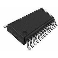
Manufacturer Part Number
PIC16LF1518-E/SS
Description
28-pin, 28KB Flash, 1024B RAM, 10-bit ADC, 2xCCP, SPI, MI2C, EUSART, 1.8V-3.6V 2
Manufacturer
Microchip Technology
Series
PIC® XLP™ 16Fr
Datasheet
1.PIC16LF1517-IPT.pdf
(344 pages)
Specifications of PIC16LF1518-E/SS
Core Processor
PIC
Core Size
8-Bit
Speed
20MHz
Connectivity
I²C, LIN, SPI, UART/USART
Peripherals
Brown-out Detect/Reset, POR, PWM, WDT
Number Of I /o
25
Program Memory Size
28KB (16K x 14)
Program Memory Type
FLASH
Ram Size
1K x 8
Voltage - Supply (vcc/vdd)
1.8 V ~ 3.6 V
Data Converters
A/D 17x10b
Oscillator Type
Internal
Operating Temperature
-40°C ~ 125°C
Package / Case
*
Processor Series
PIC16LF151x
Core
PIC
Data Bus Width
8 bit
Data Ram Size
1 KB
Interface Type
I2C, SPI, USART
Maximum Clock Frequency
20 MHz
Number Of Programmable I/os
25
Number Of Timers
3
Operating Supply Voltage
1.8 V to 3.6 V
Maximum Operating Temperature
+ 125 C
Mounting Style
SMD/SMT
Lead Free Status / RoHS Status
Lead free / RoHS Compliant
Eeprom Size
-
Lead Free Status / Rohs Status
Details


18.11 Timer1 Control Register
The Timer1 Control register (T1CON), shown in
Register
various features of the Timer1 module.
REGISTER 18-1:
2010 Microchip Technology Inc.
bit 7
Legend:
R = Readable bit
u = Bit is unchanged
‘1’ = Bit is set
bit 7-6
bit 5-4
bit 3
bit 2
bit 1
bit 0
R/W-0/u
TMR1CS<1:0>
18-1, is used to control Timer1 and select the
TMR1CS<1:0>: Timer1 Clock Source Select bits
11 = Timer1 clock source is LFINTOSC
10 = Timer1 clock source is pin or oscillator:
01 = Timer1 clock source is system clock (F
00 = Timer1 clock source is instruction clock (F
T1CKPS<1:0>: Timer1 Input Clock Prescale Select bits
11 = 1:8 Prescale value
10 = 1:4 Prescale value
01 = 1:2 Prescale value
00 = 1:1 Prescale value
T1OSCEN: LP Oscillator Enable Control bit
1 = Secondary oscillator circuit enabled for Timer1
0 = Secondary oscillator circuit disabled for Timer1
T1SYNC: Timer1 External Clock Input Synchronization Control bit
TMR1CS<1:0> = 1X
1 = Do not synchronize external clock input
0 = Synchronize external clock input with system clock (F
TMR1CS<1:0> = 0X
This bit is ignored. Timer1 uses the internal clock when TMR1CS<1:0> = 1X.
Unimplemented: Read as ‘0’
TMR1ON: Timer1 On bit
1 = Enables Timer1
0 = Stops Timer1
R/W-0/u
Clears Timer1 Gate flip-flop
If T1OSCEN = 0:
External clock from T1CKI pin (on the rising edge)
If T1OSCEN = 1:
Crystal oscillator on SOSCI/SOSCO pins
T1CON: TIMER1 CONTROL REGISTER
W = Writable bit
x = Bit is unknown
‘0’ = Bit is cleared
R/W-0/u
T1CKPS<1:0>
R/W-0/u
Preliminary
U = Unimplemented bit, read as ‘0’
-n/n = Value at POR and BOR/Value at all other Resets
OSC
T1OSCEN
R/W-0/u
OSC
)
PIC16(L)F1516/7/8/9
/4)
OSC
T1SYNC
R/W-0/u
)
U-0
—
DS41452A-page 167
TMR1ON
R/W-0/u
bit 0
Related parts for PIC16LF1518-E/SS
Image
Part Number
Description
Manufacturer
Datasheet
Request
R

Part Number:
Description:
IC, 8BIT MCU, PIC16LF, 32MHZ, QFN-28
Manufacturer:
Microchip Technology
Datasheet:

Part Number:
Description:
IC, 8BIT MCU, PIC16LF, 32MHZ, QFN-28
Manufacturer:
Microchip Technology
Datasheet:

Part Number:
Description:
IC, 8BIT MCU, PIC16LF, 32MHZ, DIP-18
Manufacturer:
Microchip Technology
Datasheet:

Part Number:
Description:
IC, 8BIT MCU, PIC16LF, 20MHZ, TQFP-44
Manufacturer:
Microchip Technology
Datasheet:
Part Number:
Description:
7 KB Flash, 384 Bytes RAM, 32 MHz Int. Osc, 16 I/0, Enhanced Mid Range Core, Nan
Manufacturer:
Microchip Technology

Part Number:
Description:
14KB Flash, 512B RAM, LCD, 11x10b ADC, EUSART, NanoWatt XLP 28 SOIC .300in T/R
Manufacturer:
Microchip Technology
Datasheet:
Part Number:
Description:
14KB Flash, 512B RAM, LCD, 11x10b ADC, EUSART, NanoWatt XLP 28 SSOP .209in T/R
Manufacturer:
Microchip Technology
Datasheet:
Part Number:
Description:
MCU PIC 14KB FLASH XLP 28-SSOP
Manufacturer:
Microchip Technology
Part Number:
Description:
MCU PIC 14KB FLASH XLP 28-SOIC
Manufacturer:
Microchip Technology
Part Number:
Description:
MCU PIC 512B FLASH XLP 28-UQFN
Manufacturer:
Microchip Technology
Part Number:
Description:
MCU PIC 14KB FLASH XLP 28-SPDIP
Manufacturer:
Microchip Technology

Part Number:
Description:
MCU 7KB FLASH 256B RAM 40-UQFN
Manufacturer:
Microchip Technology
Part Number:
Description:
MCU 7KB FLASH 256B RAM 44-TQFP
Manufacturer:
Microchip Technology

Part Number:
Description:
MCU 14KB FLASH 1KB RAM 28-UQFN
Manufacturer:
Microchip Technology
Part Number:
Description:
MCU PIC 14KB FLASH XLP 40-UQFN
Manufacturer:
Microchip Technology