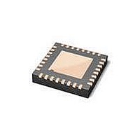
ISP1504ABS,118 NXP Semiconductors, ISP1504ABS,118 Datasheet - Page 15

ISP1504ABS,118
Manufacturer Part Number
ISP1504ABS,118
Description
RF Transceiver USB ULPI TRANSCEIVER
Manufacturer
NXP Semiconductors
Datasheet
1.ISP1504ABS118.pdf
(83 pages)
Specifications of ISP1504ABS,118
Number Of Transceivers
1
Esd Protection
YeskV
Operating Supply Voltage (typ)
Not RequiredV
Operating Temperature Classification
Industrial
Operating Supply Voltage (max)
Not RequiredV
Operating Supply Voltage (min)
Not RequiredV
Pin Count
32
Mounting
Surface Mount
Operating Temperature (max)
85C
Operating Temperature (min)
-40C
Operating Supply Voltage
1.65 V to 3.6 V
Mounting Style
SMD/SMT
Package / Case
HVQFN-32
Lead Free Status / RoHS Status
Compliant
Other names
935278308118 ISP1504ABS-T
NXP Semiconductors
ISP1504A_ISP1504C_3
Product data sheet
7.9.16 STP
7.9.17 NXT
7.9.18 CLOCK
7.9.19 CHIP_SELECT_N
7.9.20 GND (die pad)
ULPI stop input pin. The link must assert STP to signal the end of a USB transmit packet
or a register write operation. When DIR is asserted, the link can optionally assert STP to
abort the ISP1504, causing it to deassert DIR in the next clock cycle. A weak pull-up
resistor is incorporated into the STP pin as part of the interface protect feature. For details,
see
The STP input will be ignored when CHIP_SELECT_N is driven to HIGH.
For details on STP usage, refer to UTMI+ Low Pin Interface (ULPI) Specification Rev. 1.1 .
ULPI next data output pin. The ISP1504 holds NXT at LOW, by default. When DIR is LOW
and the link is sending data to the ISP1504, NXT will be asserted to notify the link to
provide the next data byte. When DIR is at HIGH and the ISP1504 is sending data to the
link, NXT will be asserted to notify the link that another valid byte is on the bus. NXT is not
used for register read data or the RXCMD status update.
The NXT pin can also be 3-stated by driving CHIP_SELECT_N to HIGH.
For details on NXT usage, refer to UTMI+ Low Pin Interface (ULPI) Specification Rev. 1.1 .
A 60 MHz interface clock to synchronize the ULPI bus. The ISP1504 provides two
clocking options:
For details on CLOCK usage, refer to UTMI+ Low Pin Interface (ULPI) Specification
Rev. 1.1 .
Active LOW chip select pin. If CHIP_SELECT_N is not used, it must be connected to
GND. For more information on using CHIP_SELECT_N, see
Global ground signal, except for the charge pump that uses CPGND. The die pad is
exposed on the underside of the package as a ground plate. This acts as a ground to all
circuits in the ISP1504, except the charge pump. To ensure correct operation of the
ISP1504, GND must be soldered to the cleanest ground available.
•
•
A crystal is attached between the XTAL1 and XTAL2 pins.
A clock is driven into the XTAL1 pin, with the XTAL2 pin left floating.
Section
9.3.1.
Rev. 03 — 7 April 2008
ISP1504A; ISP1504C
ULPI HS USB OTG transceiver
Section
9.3.3.
© NXP B.V. 2008. All rights reserved.
14 of 82


