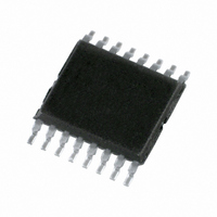
74HCT9046APW,118 NXP Semiconductors, 74HCT9046APW,118 Datasheet - Page 12

74HCT9046APW,118
Manufacturer Part Number
74HCT9046APW,118
Description
IC PLL W/BAND GAP VCO 16TSSOP
Manufacturer
NXP Semiconductors
Type
Phase Lock Loop (PLL)r
Series
74HCTr
Datasheet
1.74HCT9046AD118.pdf
(43 pages)
Specifications of 74HCT9046APW,118
Number Of Circuits
1
Package / Case
16-TSSOP
Pll
Yes
Input
Clock
Output
Clock
Ratio - Input:output
2:2
Differential - Input:output
No/No
Frequency - Max
16MHz
Divider/multiplier
No/No
Voltage - Supply
4.5 V ~ 5.5 V
Operating Temperature
-40°C ~ 125°C
Mounting Type
Surface Mount
Frequency-max
16MHz
Supply Voltage (max)
5.5 V
Supply Voltage (min)
4.5 V
Maximum Operating Temperature
+ 125 C
Minimum Operating Temperature
- 40 C
Mounting Style
SMD/SMT
Operating Supply Voltage
5 V
Lead Free Status / RoHS Status
Lead free / RoHS Compliant
Lead Free Status / RoHS Status
Lead free / RoHS Compliant, Lead free / RoHS Compliant
Other names
74HCT9046APW-T
74HCT9046APW-T
935221200118
74HCT9046APW-T
935221200118
Available stocks
Company
Part Number
Manufacturer
Quantity
Price
Company:
Part Number:
74HCT9046APW,118
Manufacturer:
CY
Quantity:
490
NXP Semiconductors
74HCT9046A_6
Product data sheet
Fig 11. The response of a locked-loop in the vicinity of the zero crossing of the phase error
(1) Due to parasitic capacitance on PC2_OUT.
(2) Backlash time (dead zone).
a. Response with traditional voltage-switch
charge-pump PC2_OUT (74HCT4046A).
VCO_IN
2.75
2.50
2.25
25
The design of the low-pass filter is somewhat different when using current sources. The
external resistor R3 is no longer present when using PC2 as phase comparator.
The current source is set by R
because the capacitor is charged by a constant current. The transfer function of the
voltage switch charge pump may be used. In fact it is even more valid, because the
transfer function is no longer restricted for small changes only. Further the current is
independent from both the supply voltage and the voltage across the filter. For one that is
familiar with the low-pass filter design of the 74HCT4046A a relation may show how R
relates with a fictive series resistance, called R3'.
This relation can be derived by assuming first that a voltage controlled switch PC2 of the
74HCT4046A is connected to the filter capacitance C2 via this fictive R3' (see
Then during the PC2 output pulse the charge current equals:
With the initial voltage V
As shown before the charge current of the current switch of the 74HCT9046A is:
Hence:
R3‘
I
I
(1)
cp
cp
=
=
=
17
R
----------- -
(2)
V
-------------------------------- -
0
17
bias
CC
phase error (ns)
----------- -
R
2.5
–
R3'
bias
V
(1)
C2 0
001aak444
Rev. 06 — 15 September 2009
25
C2(0)
at: 0.5V
bias
. A simple capacitor behaves as an ideal integrator now,
CC
b. Response with current switch charge-pump
= 2.5 V,
PC2_OUT as applied in the 74HCT9046A.
VCO_IN
2.75
2.50
2.25
I
cp
25
PLL with band gap controlled VCO
=
-------
R3'
2.5
74HCT9046A
0
phase error (ns)
© NXP B.V. 2009. All rights reserved.
001aak445
25
Figure
12 of 43
8b).
bias


