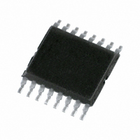
74HCT9046APW,118 NXP Semiconductors, 74HCT9046APW,118 Datasheet - Page 34

74HCT9046APW,118
Manufacturer Part Number
74HCT9046APW,118
Description
IC PLL W/BAND GAP VCO 16TSSOP
Manufacturer
NXP Semiconductors
Type
Phase Lock Loop (PLL)r
Series
74HCTr
Datasheet
1.74HCT9046AD118.pdf
(43 pages)
Specifications of 74HCT9046APW,118
Number Of Circuits
1
Package / Case
16-TSSOP
Pll
Yes
Input
Clock
Output
Clock
Ratio - Input:output
2:2
Differential - Input:output
No/No
Frequency - Max
16MHz
Divider/multiplier
No/No
Voltage - Supply
4.5 V ~ 5.5 V
Operating Temperature
-40°C ~ 125°C
Mounting Type
Surface Mount
Frequency-max
16MHz
Supply Voltage (max)
5.5 V
Supply Voltage (min)
4.5 V
Maximum Operating Temperature
+ 125 C
Minimum Operating Temperature
- 40 C
Mounting Style
SMD/SMT
Operating Supply Voltage
5 V
Lead Free Status / RoHS Status
Lead free / RoHS Compliant
Lead Free Status / RoHS Status
Lead free / RoHS Compliant, Lead free / RoHS Compliant
Other names
74HCT9046APW-T
74HCT9046APW-T
935221200118
74HCT9046APW-T
935221200118
Available stocks
Company
Part Number
Manufacturer
Quantity
Price
Company:
Part Number:
74HCT9046APW,118
Manufacturer:
CY
Quantity:
490
NXP Semiconductors
74HCT9046A_6
Product data sheet
Using PC2 with the passive filter as shown in
same performance as a loop with an active filter. Hence loop filter equations as for a high
gain loop should be used. The current source output of PC2 can be simulated then with a
fictive filter resistance:
The transfer functions of the filter is given by:
Where:
The characteristic equation is:
This results in:
or:
This can be written as:
with the natural frequency
and the damping value given as:
In
The overshoot and settling time percentages are now used to determine
From
of less than 20 % and settle to within 5 % at
This results in:
K
R3‘
K
1
s
s
2
2
1
2
+
n
p
f
Figure 35
+
+
=
=
K
=
=
=
sK
2
=
p
R3‘ C2
R4 C2
Figure 35
1
---------------- -
----------- -
4
p
R
----------- -
1
---------------- -
K
-------------------------------- -
+
s
5
K
17
n
bias
+
s
s
p
s
v
2
K
+
s
1
2
=
n
the output frequency response to a step of input frequency is shown.
K
2
---- -
1
v
0.4 V r
2
1
K
----- - K
n
it can be seen that the damping ratio = 0.707 will produce an overshoot
s
+
v
2
K
K
=
n
n
p
Rev. 06 — 15 September 2009
K
0
=
v
0
K
n
n
1
defined as:
=
1
0
+
K
=
p
0.5
K
f
2
K
Figure 34
n
o
t = 5. The required settling time is 1 ms.
n
K
n
PLL with band gap controlled VCO
results in a high gain loop with the
74HCT9046A
© NXP B.V. 2009. All rights reserved.
n
.
34 of 43


