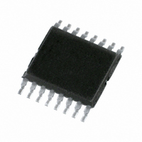
74HCT9046APW,118 NXP Semiconductors, 74HCT9046APW,118 Datasheet - Page 15

74HCT9046APW,118
Manufacturer Part Number
74HCT9046APW,118
Description
IC PLL W/BAND GAP VCO 16TSSOP
Manufacturer
NXP Semiconductors
Type
Phase Lock Loop (PLL)r
Series
74HCTr
Datasheet
1.74HCT9046AD118.pdf
(43 pages)
Specifications of 74HCT9046APW,118
Number Of Circuits
1
Package / Case
16-TSSOP
Pll
Yes
Input
Clock
Output
Clock
Ratio - Input:output
2:2
Differential - Input:output
No/No
Frequency - Max
16MHz
Divider/multiplier
No/No
Voltage - Supply
4.5 V ~ 5.5 V
Operating Temperature
-40°C ~ 125°C
Mounting Type
Surface Mount
Frequency-max
16MHz
Supply Voltage (max)
5.5 V
Supply Voltage (min)
4.5 V
Maximum Operating Temperature
+ 125 C
Minimum Operating Temperature
- 40 C
Mounting Style
SMD/SMT
Operating Supply Voltage
5 V
Lead Free Status / RoHS Status
Lead free / RoHS Compliant
Lead Free Status / RoHS Status
Lead free / RoHS Compliant, Lead free / RoHS Compliant
Other names
74HCT9046APW-T
74HCT9046APW-T
935221200118
74HCT9046APW-T
935221200118
Available stocks
Company
Part Number
Manufacturer
Quantity
Price
Company:
Part Number:
74HCT9046APW,118
Manufacturer:
CY
Quantity:
490
NXP Semiconductors
10. Recommended operating conditions
Table 4.
11. Static characteristics
Table 5.
At recommended operating conditions; voltages are referenced to GND (ground = 0 V).
74HCT9046A_6
Product data sheet
Symbol
V
V
V
T
Symbol
T
Phase comparator section
V
V
V
V
I
I
R
R
I
VCO section
V
V
I
OZ
cp
amb
t/ V
amb
CC
I
O
IH
IL
OH
OL
IH
IL
I
bias
= 25 C
Operating conditions
Static characteristics
Parameter
HIGH-level input voltage
LOW-level input voltage
HIGH-level output voltage
LOW-level output voltage
input leakage current
OFF-state output current
input resistance
bias resistance
charge pump current
HIGH-level input voltage
LOW-level input voltage
Parameter
supply voltage
input voltage
output voltage
ambient temperature
input transition rise and fall rate
Rev. 06 — 15 September 2009
Conditions
pins SIG_IN and COMP_IN;
V
pins SIG_IN and COMP_IN;
V
pins PCP_OUT and PCn_OUT;
V
pins PCP_OUT and PCn_OUT;
V
pins SIG_IN and COMP_IN;
V
pin PC2_OUT; V
V
SIG_IN and COMP_IN;
V
operating point; V
see
V
V
pin INH; V
DC coupled
pin INH; V
DC coupled
CC
CC
CC
CC
CC
I
CC
CC
CC
I
I
I
I
= V
O
O
O
O
Figure
= 4.5 V; DC coupled
= 4.5 V; DC coupled
= 4.5 V; V
= 4.5 V; V
= 5.5 V; V
= 4.5 V; V
= 4.5 V
= 4.5 V; R
= 20 A
= 4.0 mA
= 20 A
= 4.0 mA
IH
or V
Conditions
pin INH; V
CC
CC
14,
IL
= 4.5 V to 5.5 V;
= 4.5 V to 5.5 V;
; V
I
I
I
I
bias
15
= V
= V
= V
at self-bias
O
CC
and
= 40 k
= V
CC
IH
IH
CC
I
= 5.5 V;
= 0.5 V;
or V
or V
= 4.5 V
or GND
CC
16
or GND
IL
IL
PLL with band gap controlled VCO
Min
4.5
0
0
-
40
74HCT9046A
Min
3.15
-
4.4
3.98
-
-
-
-
-
25
2.0
-
0.53
Typ
5.0
-
-
1.67
Typ
2.4
2.1
4.5
4.32
0
0.15
-
-
250
-
1.6
1.2
1.06
© NXP B.V. 2009. All rights reserved.
Max
5.5
V
V
+125
139
CC
CC
Max
-
1.35
-
-
0.1
0.26
-
250
-
0.8
30
0.5
2.12 mA
Unit
V
V
V
ns/V
C
15 of 43
Unit
V
V
V
V
V
V
k
k
V
V
A
A


