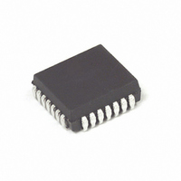
MC88LV915TFN Freescale Semiconductor, MC88LV915TFN Datasheet - Page 4

MC88LV915TFN
Manufacturer Part Number
MC88LV915TFN
Description
IC DRV CLK PLL LV 100MHZ 28-PLCC
Manufacturer
Freescale Semiconductor
Type
Clock Driver, Fanout Distribution, Multiplexerr
Datasheet
1.MC88LV915TFN.pdf
(12 pages)
Specifications of MC88LV915TFN
Pll
Yes
Input
TTL
Output
CMOS, TTL
Number Of Circuits
1
Ratio - Input:output
3:8
Differential - Input:output
No/No
Frequency - Max
100MHz
Divider/multiplier
Yes/Yes
Voltage - Supply
3 V ~ 3.6 V
Operating Temperature
0°C ~ 70°C
Mounting Type
Surface Mount
Package / Case
28-PLCC
Frequency-max
100MHz
Lead Free Status / RoHS Status
Contains lead / RoHS non-compliant
Available stocks
Company
Part Number
Manufacturer
Quantity
Price
Company:
Part Number:
MC88LV915TFN
Manufacturer:
Freescale Semiconductor
Quantity:
10 000
Part Number:
MC88LV915TFN
Manufacturer:
FREESCALE
Quantity:
20 000
Company:
Part Number:
MC88LV915TFNR2
Manufacturer:
Freescale Semiconductor
Quantity:
10 000
MAXIMUM RATINGS*
* Maximum Ratings are those values beyond which damage to the device may occur. Functional operation should be restricted to the Recommended
Operating Conditions.
RECOMMENDED OPERATING CONDITIONS
DC CHARACTERISTICS (T
1. I
2. The PLL_EN input pin is not guaranteed to meet this specification.
3. Maximum test duration 2.0ms, one output loaded at a time.
SYNC INPUT TIMING REQUIREMENTS
V
V
V
I
I
I
T
V
V
V
T
ESD
V
V
V
V
I
I
I
I
I
t
SYNC Input
t
SYNC Input
Duty Cycle
Symbol
in
out
CC
IN
CCT
OLD
OHD
CC
RISE/FALL
CYCLE
4
stg
A
CC
in
out
CC
in
out
IH
IL
OH
OL
OL
Symbol
Symbol
, AV
is +12mA for the RST_OUT output.
Symbol
,
CC
Minimum High Level Input Voltage
Minimum Low Level Input Voltage
Minimum High Level Output Voltage
Minimum Low Level Output Voltage
Maximum Input Leakage Current
Maximum I
Minimum Dynamic
Maximum Quiescent Supply Current
DC Supply Voltage Referenced to GND
DC Input Voltage (Referenced to GND)
DC Output Voltage (Referenced to GND)
DC Input Current, Per Pin
DC Output Sink/Source Current, Per Pin
DC V
Storage Temperature
Supply Voltage
DC Input Voltage
DC Output Voltage
Ambient Operating Temperature
Static Discharge Voltage
Rise/Fall Time, SYNC Input
From 0.8V to 2.0V
Input Clock Period
SYNC Input
Duty Cycle, SYNC Input
CC
CC
Parameter
/Input
or GND Current Per Output Pin
A
= 0 C to 70 C; V
3
Output Current
CC
Parameter
Parameter
= 3.3V
Parameter
V
3.0
3.3
3.0
3.3
3.0
3.3
3.0
3.3
3.6
3.6
3.6
3.6
3.6
CC
0.3V)
Guaranteed Limits
0.44
0.44
TBD
+50
–50
2.0
2.0
0.8
0.8
2.4
2.7
2.0
1.0
Minimum
f 2X_Q 4
Unit
mA
mA
mA
V
V
V
V
A
A
—
1
50%
–0.5 to V
–0.5 to V
–65 to +150
–0.5 to 7.0
V
V
V
V
V
I
V
I
V
V
V
V
V
OH
OH
0 to V
0 to V
3.3 0.3
OUT
CC
OUT
CC
IN
IN
I
I
OLD
OHD
I
Limits
Limits
0 to 70
> 1000
= V
= V
= V
= –24mA
= 24mA
25%
= V
= V
20
50
50
– 0.1V
– 0.1V
CC
CC
Maximum
= 0.1V or
= 0.1V or
= 1.25V
CC
CC
CC
=2.35V
CC
CC
IH
IH
Condition
, GND
, GND
100
+0.5
+0.5
5.0
– 2.1V
or V
or V
IL
IL
MOTOROLA
Unit
ns
ns
Unit
Unit
mA
mA
mA
V
V
V
V
V
V
V
C
C


