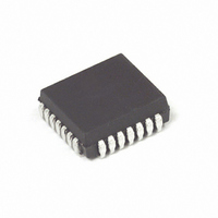
MC88LV915TFN Freescale Semiconductor, MC88LV915TFN Datasheet - Page 9

MC88LV915TFN
Manufacturer Part Number
MC88LV915TFN
Description
IC DRV CLK PLL LV 100MHZ 28-PLCC
Manufacturer
Freescale Semiconductor
Type
Clock Driver, Fanout Distribution, Multiplexerr
Datasheet
1.MC88LV915TFN.pdf
(12 pages)
Specifications of MC88LV915TFN
Pll
Yes
Input
TTL
Output
CMOS, TTL
Number Of Circuits
1
Ratio - Input:output
3:8
Differential - Input:output
No/No
Frequency - Max
100MHz
Divider/multiplier
Yes/Yes
Voltage - Supply
3 V ~ 3.6 V
Operating Temperature
0°C ~ 70°C
Mounting Type
Surface Mount
Package / Case
28-PLCC
Frequency-max
100MHz
Lead Free Status / RoHS Status
Contains lead / RoHS non-compliant
Available stocks
Company
Part Number
Manufacturer
Quantity
Price
Company:
Part Number:
MC88LV915TFN
Manufacturer:
Freescale Semiconductor
Quantity:
10 000
Part Number:
MC88LV915TFN
Manufacturer:
FREESCALE
Quantity:
20 000
Company:
Part Number:
MC88LV915TFNR2
Manufacturer:
Freescale Semiconductor
Quantity:
10 000
MC88LV915T System Level Testing Functionality
OE/RST pin low will put all outputs (except for LOCK) into the high impedance state. As long as the PLL_EN pin is low, the
Q0–Q4, Q5, and the Q/2 outputs will remain reset in the low state after the OE/RST until a falling SYNC edge is seen. The
2X_Q output will be the inverse of the SYNC signal in this mode. If the 3–state functionality will be used, a pull–up or pull–
down resistor must be tied to the FEEDBACK input pin to prevent it from floating when the fedback output goes into high
impedance.
and disabling the VCO. In this mode the outputs are directly driven by the SYNC input (per the block diagram). This mode can
also be used for low frequency board testing.
will take a maximum of 10mS (tLOCK spec) to regain phase–lock after the OE/RST pin goes back high.
MOTOROLA
3–state functionality has been added to the 100MHz version of the MC88LV915T to ease system board testing. Bringing the
With the PLL_EN pin low the selected SYNC signal is gated directly into the internal clock distribution network, bypassing
Note: If the outputs are put into 3–state during normal PLL operation, the loop will be broken and phase–lock will be lost. It
Figure 4. Representation of a Potential Multi–Processing Application Utilizing the MC88LV915T
for Frequency Multiplication and Low Board–to–Board Skew
9


