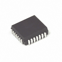
MC88LV915TFN Freescale Semiconductor, MC88LV915TFN Datasheet - Page 8

MC88LV915TFN
Manufacturer Part Number
MC88LV915TFN
Description
IC DRV CLK PLL LV 100MHZ 28-PLCC
Manufacturer
Freescale Semiconductor
Type
Clock Driver, Fanout Distribution, Multiplexerr
Datasheet
1.MC88LV915TFN.pdf
(12 pages)
Specifications of MC88LV915TFN
Pll
Yes
Input
TTL
Output
CMOS, TTL
Number Of Circuits
1
Ratio - Input:output
3:8
Differential - Input:output
No/No
Frequency - Max
100MHz
Divider/multiplier
Yes/Yes
Voltage - Supply
3 V ~ 3.6 V
Operating Temperature
0°C ~ 70°C
Mounting Type
Surface Mount
Package / Case
28-PLCC
Frequency-max
100MHz
Lead Free Status / RoHS Status
Contains lead / RoHS non-compliant
Available stocks
Company
Part Number
Manufacturer
Quantity
Price
Company:
Part Number:
MC88LV915TFN
Manufacturer:
Freescale Semiconductor
Quantity:
10 000
Part Number:
MC88LV915TFN
Manufacturer:
FREESCALE
Quantity:
20 000
Company:
Part Number:
MC88LV915TFNR2
Manufacturer:
Freescale Semiconductor
Quantity:
10 000
1. Figure 3 shows a loop filter and analog isolation scheme
1a.All loop filter and analog isolation components should be
1b.The 47
8
which will be effective in most applications. The following
guidelines should be followed to ensure stable and
jitter–free operation:
tied as close to the package as possible. Stray current
passing through the parasitics of long traces can cause
undesirable voltage transients at the RC1 pin.
capacitor, and the 0.1 F high frequency bypass capacitor
form a wide bandwidth filter that will minimize the
88LV915T’s sensitivity to voltage transients from the
system digital V
typically ensure that a 100mV step deviation on the digital
V
deviation on the 88LV915T outputs. A 250mV step
deviation on V
should cause no more than a 250pS phase deviation; if a
25 F bypass capacitor is used (instead of 10 F) a 250mV
V
deviation.
If good bypass techniques are used on a board design
near components which may cause digital V
noise, the above described V
occur at the 88LV915T’s digital V
CC
CC
step should cause no more than a 100pS phase
supply will cause no more than a 100pS phase
resistors, the 10 F low frequency bypass
Figure 3. Recommended Loop Filter and Analog Isolation Scheme for the MC88LV915T
CC
CC
supply and ground planes. This filter will
using the recommended filter values
CC
Notes Concerning Loop Filter and Board Layout Issues
step deviations should not
CC
supply. The purpose
CC
and ground
1c.There are no special requirements set forth for the loop
1d.The 1M reference resistor injects current into the internal
2. In addition to the bypass capacitors used in the analog filter
of the bypass filtering scheme shown in Figure 3 is to give
the 88LV915T additional protection from the power supply
and ground plane transients that can occur in a high
frequency, high speed digital system.
filter resistors (1M
(0.1 F) can be a ceramic chip capacitior, the same as a
standard bypass capacitor.
charge pump of the PLL, causing a fixed offset between
the outputs and the SYNC input. This also prevents
excessive jitter caused by inherent PLL dead–band. If the
VCO (2X_Q output) is running above 40MHz, the 1M
resistor provides the correct amount of current injection
into the charge pump (2–3 A). For the TFN55, 70 or 100,
if the VCO is running below 40MHz, a 1.5M
resistor should be used (instead of 1M ).
of Figure 3, there should be a 0.1 F bypass capacitor
between each of the other (digital) four V
board ground plane. This will reduce output switching
noise caused by the 88LV915T outputs, in addition to
reducing potential for noise in the ‘analog’ section of the
chip. These bypass capacitors should also be tied as close
to the 88LV915T package as possible.
and 330 ). The loop filter capacitor
CC
MOTOROLA
pins and the
reference


