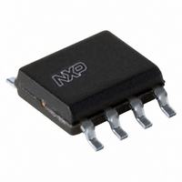
ICM7555ID/01,118 NXP Semiconductors, ICM7555ID/01,118 Datasheet - Page 12

ICM7555ID/01,118
Manufacturer Part Number
ICM7555ID/01,118
Description
IC CMOS TIMER GEN-PURPOSE 8-SOIC
Manufacturer
NXP Semiconductors
Type
555 Type, Timer/Oscillator (Single)r
Specifications of ICM7555ID/01,118
Package / Case
8-SOIC (3.9mm Width)
Frequency
500kHz
Voltage - Supply
3 V ~ 16 V
Current - Supply
180µA
Operating Temperature
-40°C ~ 85°C
Number Of Internal Timers
1
Supply Voltage (max)
16 V
Supply Voltage (min)
3 V
Maximum Power Dissipation
780 mW
Maximum Operating Temperature
+ 85 C
Minimum Operating Temperature
- 40 C
Mounting Style
SMD/SMT
Supply Current
80 uA
Lead Free Status / RoHS Status
Lead free / RoHS Compliant
Count
-
Lead Free Status / Rohs Status
Lead free / RoHS Compliant
Other names
568-1820-2
935274819118
ICM7555ID/01-T
935274819118
ICM7555ID/01-T
NXP Semiconductors
ICM7555_2
Product data sheet
11.4 Astable operation
11.5 Monostable operation
If the circuit is connected as shown in
multivibrator. The external capacitor charges through R
R
this mode of operation, the capacitor charges and discharges between
2
supply voltage, the frequency of oscillation is independent of the supply voltage.
In this mode of operation, the timer functions as a one-shot. Initially, the external
capacitor (C) is held discharged by a transistor inside the timer. Upon application of a
negative pulse to pin 2, TRIGGER, the internal flip-flop is set, which releases the
low-impedance on DISCHARGE; the external capacitor charges and drives the OUTPUT
HIGH. The voltage across the capacitor increases exponentially with a time constant
t = R
flip-flop, which in turn discharges the capacitor rapidly and also drives the OUTPUT to its
LOW state. TRIGGER must return to a HIGH state before the OUTPUT can return to a
LOW state.
f
3
Fig 15. Astable operation
B
=
=
V
only. Thus, the duty cycle ( ) may be precisely set by the ratio of these two resistors. In
DD
A
---------------------- -
R
------------------------------------- -
R
C. When the voltage across the capacitor equals
R
A
. Since the charge rate and the threshold levels are directly proportional to the
A
A
+
+
+
2R
1.38
R
2R
OUTPUT
B
B
B
C
Rev. 02 — 3 August 2009
V
DD
R A
R B
C
V
DD
1
2
3
4
Figure
GND
TRIGGER
OUTPUT
RESET
15, it will trigger itself and free run as a
CONTROL_VOLTAGE
THRESHOLD
DISCHARGE
A
2
3
and R
General purpose CMOS timer
V+, the comparator resets the
V
DD
B
and discharges through
8
7
6
5
© NXP B.V. 2009. All rights reserved.
ICM7555
1
002aae418
3
V
V
DD
DD
and
12 of 22
(1)
(2)


