HSP45116AVC-52Z Intersil, HSP45116AVC-52Z Datasheet - Page 7
HSP45116AVC-52Z
Manufacturer Part Number
HSP45116AVC-52Z
Description
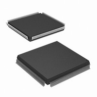
IC OSCILLATOR/MOD NCO 160-MQFP
Manufacturer
Intersil
Type
Numerically Controlled Oscillator (NCO)r
Datasheet
1.HSP45116AVC-52Z.pdf
(19 pages)
Specifications of HSP45116AVC-52Z
Frequency
52MHz
Voltage - Supply
4.75 V ~ 5.25 V
Current - Supply
184mA
Operating Temperature
0°C ~ 70°C
Package / Case
160-MQFP, 160-PQFP
Lead Free Status / RoHS Status
Lead free / RoHS Compliant
Count
-
Available stocks
Company
Part Number
Manufacturer
Quantity
Price


Functional Description
The Numerically Controlled Oscillator/Modulator (NCOM)
produces a digital complex sinusoid waveform whose
amplitude, phase and frequency are controlled by a set of
input command words. When used as a Numerically
Controlled Oscillator (NCO), it generates 16-bit sine and
cosine vectors at a maximum sample rate of 40MHz. The
NCOM can be preprogrammed to produce a constant (CW)
sine and cosine output for Direct Digital Synthesis (DDS)
applications. Alternatively, the phase and frequency inputs
can be updated in real time to produce a FM, PSK, FSK, or
MSK modulated waveform. The Complex Multiplier/
Accumulator (CMAC) can be used to multiply this waveform
by an input signal for AM and QAM signals. By stepping the
phase input, the output of the ROM becomes an FFT twiddle
factor; when data is input to the Vector Inputs (see Block
Diagram), the NCOM calculates an FFT butterfly.
As shown in the Block Diagram, the NCOM consists of
three parts: Phase and Frequency Control Section (PFCS),
Sine/Cosine Generator, and CMAC. The PFCS stores the
phase and frequency inputs and uses them to calculate the
phase angle of a rotating complex vector. The Sine/Cosine
Generator performs a lookup on this phase and outputs the
appropriate values for the sine and cosine. The sine and
cosine form one set of inputs to the CMAC, which multiplies
them by the input vector to form the modulated output.
The outputs of the CMAC and ACC can be rounded to
different bit widths.
Phase and Frequency Control Section
The phase and frequency of the internally generated sine
and cosine are controlled by the PFCS (Figure 1). The PFCS
generates a 32-bit word that represents the current phase of
the sine and cosine waves being generated: The Sine/
Cosine Argument. Stepping this phase angle from 0 through
full scale (2
sinusoid starting at 0
counterclockwise. The PFCS automatically increments the
phase by a preprogrammed amount on every rising edge of
the external clock. The value of the phase step (which is the
sum of the Center and Offset Frequency Registers) is:
Phase Step =
where Signal Frequency is a 2’s complement number. The
sign bit will set the output vector notation for Upper Sideband
(USB) or lower Sideband (LSB) applications.
The PFCS is divided into two sections: The Phase
Accumulator uses the data on C0-15 to compute the phase
angle, that is the input to the Sine/Cosine Section (Sine/
Cosine Argument); the Time Accumulator supplies a pulse to
mark the passage of a preprogrammed period of time.
32
Signal Frequency
--------------------------------------------- -
Clock Frequency
- 1) corresponds to the phase angle of a
o
and advancing around the unit circle
×
7
2
32
HSP45116A
The Phase Accumulator and Time Accumulator work on the
same principle: a 32-bit word is added to the contents of a
32-bit accumulator register every clock cycle; when the sum
causes the adder to overflow, the accumulation continues
with the 32 bits of the adder going into the Accumulator
Register. The overflow bit is used as an output to indicate
the timing of the accumulation overflows. In the Time
Accumulator, the overflow bit generates TICO, the Time
Accumulator carry out (which is the only output of the Time
Accumulator). In the Phase Accumulator, the overflow is
inverted to generate the Phase Accumulator Carry Out,
PACO.
The output of the Phase Accumulator goes to the Phase
Adder, which adds an offset to the top 16 bits of the phase.
This 32-bit number forms the argument of the sine and
cosine, which is passed to the Sine/Cosine Generator.
Both accumulators are loaded 16 bits at a time over the
C0-15 bus. Data on C0-15 is loaded into one of the three
input registers when CS and WR are low. The data in the
Most Significant Input Register and Least Significant Input
Register forms a 32-bit word that is the input to the Center
Frequency Register, Offset Frequency Register and Time
Accumulator. These registers are loaded by enabling the
proper register enable signal; for example, to load the
Center Frequency Register, the data is loaded into the LS
and MS Input Registers, and ENCFREG is set to zero; the
next rising edge of CLK will pass the registered version of
ENCFREG, R.ENCFREG, to the clock enable of the Center
Frequency Register; this register then gets loaded on the
following rising edge of CLK. The contents of the Input
Registers will be continuously loaded into the Center
Frequency Register as long as R.ENCFREG is low.
The Phase Register is loaded in a similar manner. Assuming
PMSEL is high, the contents of the Phase Input Register is
loaded into the Phase Register on every rising clock edge
that R.ENPHREG is low. If PMSEL is low, MOD0-1 supply
the two most significant bits into the Phase Register (MOD1
is the MSB) and the least significant 14 bits are loaded with
0. MOD0-1 and are used to generate a Quad Phase Shift
Keying (QPSK) signal (Table 2).
AD1
X
0
0
1
1
AD0
X
0
1
0
1
TABLE 1. AD0-1 DECODING
CS
0
0
0
X
1
WR
↑
↑
↑
X
X
Load least significant bits
of frequency input.
Load most significant bits
of frequency input.
Load phase register.
Reserved.
No Operation.
FUNCTION
May 7, 2007
FN4156.4
Related parts for HSP45116AVC-52Z
Image
Part Number
Description
Manufacturer
Datasheet
Request
R

Part Number:
Description:
Numerically Controlled Oscillator/modulator
Manufacturer:
Intersil Corporation
Datasheet:
Part Number:
Description:
HSP45116 Daughter Board
Manufacturer:
Intersil Corporation
Datasheet:

Part Number:
Description:
Numerically Controlled Oscillator/Modulator
Manufacturer:
INTERSIL [Intersil Corporation]
Datasheet:
Part Number:
Description:
Numerically Controlled Oscillator/modulator
Manufacturer:
Intersil Corporation
Datasheet:
Part Number:
Description:
Intersil Corporation [CMOS Serial Controller Interface]
Manufacturer:
Intersil Corporation
Datasheet:
Part Number:
Description:
Manufacturer:
Intersil Corporation
Datasheet:
Part Number:
Description:
357-036-542-201 CARDEDGE 36POS DL .156 BLK LOPRO
Manufacturer:
Intersil Corporation
Datasheet:
Part Number:
Description:
1024-Word x 4-Bit LSI Static RAM
Manufacturer:
Intersil Corporation
Datasheet:
Part Number:
Description:
General Purpose NPN Transistor Arrays FN341.4
Manufacturer:
Intersil Corporation
Datasheet:
Part Number:
Description:
CMOS 16-Bit Microprocessor
Manufacturer:
Intersil Corporation
Datasheet:
Part Number:
Description:
Manufacturer:
Intersil Corporation
Datasheet:
Part Number:
Description:
Manufacturer:
Intersil Corporation
Datasheet:
Part Number:
Description:
Manufacturer:
Intersil Corporation
Datasheet:
Part Number:
Description:
Manufacturer:
Intersil Corporation
Datasheet:
Part Number:
Description:
CMOS 6-Bit Latch and Decoder Memory Interfaces
Manufacturer:
Intersil Corporation
Datasheet: