ADC1004S030TS/C1:1 NXP Semiconductors, ADC1004S030TS/C1:1 Datasheet - Page 4
ADC1004S030TS/C1:1
Manufacturer Part Number
ADC1004S030TS/C1:1
Description
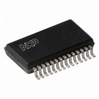
IC ADC 10BIT PAR 30MHZ 28-SSOP
Manufacturer
NXP Semiconductors
Datasheet
1.ADC1004S030TSC11.pdf
(19 pages)
Specifications of ADC1004S030TS/C1:1
Number Of Bits
10
Sampling Rate (per Second)
30M
Number Of Converters
1
Power Dissipation (max)
247mW
Voltage Supply Source
Analog and Digital
Operating Temperature
-40°C ~ 85°C
Mounting Type
Surface Mount
Package / Case
28-SSOP (0.200", 5.30mm Width)
Lead Free Status / RoHS Status
Lead free / RoHS Compliant
Other names
568-4430
568-4430-5
568-4430-5
935286611151
ADC1004S030TS/C1
ADC1004S030TS/C1-S
568-4430-5
568-4430-5
935286611151
ADC1004S030TS/C1
ADC1004S030TS/C1-S


NXP Semiconductors
7. Pinning information
ADC1004S030_040_050_3
Product data sheet
7.1 Pinning
7.2 Pin description
Table 3.
Symbol
CLK
TC
V
AGND
n.c.
RB
RM
VI
RT
OE
V
DGND2
V
OGND
n.c.
D0
D1
D2
D3
Fig 2.
CCA
CCD2
CCO
Pin configuration
Pin description
Pin
1
2
3
4
5
6
7
8
9
10
11
12
13
14
15
16
17
18
19
Rev. 03 — 7 August 2008
DGND2
V
OGND
AGND
V
V
CCD2
Description
clock input
two’s complement input (active LOW)
analog supply voltage (5 V)
analog ground
not connected
reference voltage BOTTOM input
reference voltage MIDDLE
analog input voltage
reference voltage TOP input
output enable input (CMOS level input, active LOW)
digital supply voltage 2 (5 V)
digital ground 2
supply voltage for output stages (3 V to 5 V)
output ground
not connected
data output; bit 0 (Least Significant Bit (LSB))
data output; bit 1
data output; bit 2
data output; bit 3
CLK
CCO
CCA
TC
n.c.
RM
RB
OE
RT
V
I
Single 10 bits ADC, up to 30 MHz, 40 MHz or 50 MHz
10
11
12
13
14
1
2
3
4
5
6
7
8
9
ADC1004S
ADC1004S030/040/050
050TS
014aaa337
28
27
26
25
24
23
22
21
20
19
18
17
16
15
V
DGND1
IR
D9
D8
D7
D6
D5
D4
D3
D2
D1
D0
n.c.
CCD1
© NXP B.V. 2008. All rights reserved.
4 of 19
Related parts for ADC1004S030TS/C1:1
Image
Part Number
Description
Manufacturer
Datasheet
Request
R

Part Number:
Description:
Single 10 Bits Adc, Up To 30 Mhz, 40 Mhz Or 50 Mhz
Manufacturer:
NXP Semiconductors
Datasheet:
Part Number:
Description:
(ADC1004S030 - ADC1004S050) Single 10 bits ADC
Manufacturer:
NXP Semiconductors
Datasheet:
Part Number:
Description:
NXP Semiconductors designed the LPC2420/2460 microcontroller around a 16-bit/32-bitARM7TDMI-S CPU core with real-time debug interfaces that include both JTAG andembedded trace
Manufacturer:
NXP Semiconductors
Datasheet:

Part Number:
Description:
NXP Semiconductors designed the LPC2458 microcontroller around a 16-bit/32-bitARM7TDMI-S CPU core with real-time debug interfaces that include both JTAG andembedded trace
Manufacturer:
NXP Semiconductors
Datasheet:
Part Number:
Description:
NXP Semiconductors designed the LPC2468 microcontroller around a 16-bit/32-bitARM7TDMI-S CPU core with real-time debug interfaces that include both JTAG andembedded trace
Manufacturer:
NXP Semiconductors
Datasheet:
Part Number:
Description:
NXP Semiconductors designed the LPC2470 microcontroller, powered by theARM7TDMI-S core, to be a highly integrated microcontroller for a wide range ofapplications that require advanced communications and high quality graphic displays
Manufacturer:
NXP Semiconductors
Datasheet:
Part Number:
Description:
NXP Semiconductors designed the LPC2478 microcontroller, powered by theARM7TDMI-S core, to be a highly integrated microcontroller for a wide range ofapplications that require advanced communications and high quality graphic displays
Manufacturer:
NXP Semiconductors
Datasheet:
Part Number:
Description:
The Philips Semiconductors XA (eXtended Architecture) family of 16-bit single-chip microcontrollers is powerful enough to easily handle the requirements of high performance embedded applications, yet inexpensive enough to compete in the market for hi
Manufacturer:
NXP Semiconductors
Datasheet:
Part Number:
Description:
The XA-S3 device is a member of Philips Semiconductors? XA(eXtended Architecture) family of high performance 16-bitsingle-chip microcontrollers
Manufacturer:
NXP Semiconductors
Datasheet:

Part Number:
Description:
The NXP BlueStreak LH75401/LH75411 family consists of two low-cost 16/32-bit System-on-Chip (SoC) devices
Manufacturer:
NXP Semiconductors
Datasheet:
Part Number:
Description:
The NXP LPC3130/3131 combine an 180 MHz ARM926EJ-S CPU core, high-speed USB2
Manufacturer:
NXP Semiconductors
Datasheet:
Part Number:
Description:
The NXP LPC3141 combine a 270 MHz ARM926EJ-S CPU core, High-speed USB 2
Manufacturer:
NXP Semiconductors
Part Number:
Description:
The NXP LPC3143 combine a 270 MHz ARM926EJ-S CPU core, High-speed USB 2
Manufacturer:
NXP Semiconductors