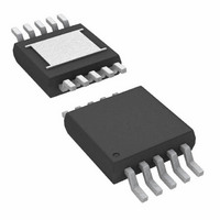
LTC1403ACMSE Linear Technology, LTC1403ACMSE Datasheet - Page 10

LTC1403ACMSE
Manufacturer Part Number
LTC1403ACMSE
Description
IC ADC 14BIT 2.8MSPS DIFF 10MSOP
Manufacturer
Linear Technology
Datasheet
1.LTC1403CMSEPBF.pdf
(20 pages)
Specifications of LTC1403ACMSE
Number Of Bits
14
Sampling Rate (per Second)
2.8M
Data Interface
Serial, SPI™
Number Of Converters
1
Power Dissipation (max)
12mW
Voltage Supply Source
Single Supply
Operating Temperature
0°C ~ 70°C
Mounting Type
Surface Mount
Package / Case
10-TFSOP, 10-MSOP (0.118", 3.00mm Width) Exposed Pad
Lead Free Status / RoHS Status
Contains lead / RoHS non-compliant
Available stocks
Company
Part Number
Manufacturer
Quantity
Price
Company:
Part Number:
LTC1403ACMSE
Manufacturer:
LT
Quantity:
10 000
Part Number:
LTC1403ACMSE#PBF
Manufacturer:
LINEAR/凌特
Quantity:
20 000
Company:
Part Number:
LTC1403ACMSE#TRPBF
Manufacturer:
SONY
Quantity:
101
Part Number:
LTC1403ACMSE#TRPBF
Manufacturer:
LINEAR/凌特
Quantity:
20 000
Company:
Part Number:
LTC1403ACMSE-1
Manufacturer:
LT
Quantity:
10 000
Company:
Part Number:
LTC1403ACMSE-1#TRPBF
Manufacturer:
LT
Quantity:
2 300
APPLICATIONS INFORMATION
LTC1403/LTC1403A
INPUT FILTERING AND SOURCE IMPEDANCE
The noise and the distortion of the input amplifi er and other
circuitry must be considered since they will add to the
LTC1403/LTC1403A noise and distortion. The small-signal
bandwidth of the sample-and-hold circuit is 50MHz. Any
noise or distortion products that are present at the analog
inputs will be summed over this entire bandwidth. Noisy
input circuitry should be fi ltered prior to the analog inputs
to minimize noise. A simple 1-pole RC fi lter is suffi cient for
many applications. For example, Figure 1 shows a 47pF
capacitor from A
limit the input bandwidth to 47MHz. The 47pF capacitor also
acts as a charge reservoir for the input sample-and-hold
and isolates the ADC input from sampling-glitch sensitive
circuitry. High quality capacitors and resistors should be
used since these components can add distortion. NPO
and silvermica type dielectric capacitors have excellent
linearity. Carbon surface mount resistors can generate
distortion from self heating and from damage that may
occur during soldering. Metal fi lm surface mount resistors
are much less susceptible to both problems. When high
amplitude unwanted signals are close in frequency to the
desired signal frequency, a multiple pole fi lter is required.
High external source resistance, combined with the 13pF of
input capacitance, will reduce the rated 50MHz bandwidth
and increase acquisition time beyond 39ns.
10
IN
51Ω
Figure 1. RC Input Filter
+
to ground and a 51Ω source resistor to
10μF
47pF
11
1
2
3
A
A
V
GND
IN
IN
REF
LTC1403A
+
–
LTC1403/
1403A F01
INPUT RANGE
The analog inputs of the LTC1403/LTC1403A may be
driven fully differentially with a single supply. Each input
may swing up to 3V
range, the noninverting input of each channel is always
up to 2.5V more positive than the inverting input of each
channel. The 0V to 2.5V range is also ideally suited for
single-ended input use with single supply applications. The
common mode range of the inputs extend from ground
to the supply voltage V
A
stay fi xed at all ones and if this difference goes below 0V,
the ouput code will stay fi xed at all zeros.
INTERNAL REFERENCE
The LTC1403/LTC1403A has an on-chip, temperature
compensated, bandgap reference that is factory trimmed
near 2.5V to obtain 2.5V input span. The reference amplifi er
output V
ground. The reference amplifi er is stable with capacitors
of 1μF or greater. For the best noise performance, a 10μF
ceramic or a 10μF tantalum in parallel with a 0.1μF ceramic
is recommended. The V
external reference as shown in Figure 2. The voltage of
the external reference must be higher than the 2.5V of the
class A pull-up output of the internal reference. The recom-
mended range for an external reference is 2.55V to V
An external reference at 2.55V will see a DC quiescent load
of 0.75mA and as much as 3mA during conversion.
IN
+
and A
REF
IN
, (Pin 3) must be bypassed with a capacitor to
–
inputs exceeds 2.5V, the output code will
3V
REF
P-P
10μF
DD
REF
Figure 2
individually. In the conversion
. If the difference between the
pin can be overdriven with an
11
3
V
GND
REF
LTC1403A
LTC1403/
1403A F02
1403fb
DD
.


