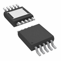
LTC1403ACMSE Linear Technology, LTC1403ACMSE Datasheet - Page 13

LTC1403ACMSE
Manufacturer Part Number
LTC1403ACMSE
Description
IC ADC 14BIT 2.8MSPS DIFF 10MSOP
Manufacturer
Linear Technology
Datasheet
1.LTC1403CMSEPBF.pdf
(20 pages)
Specifications of LTC1403ACMSE
Number Of Bits
14
Sampling Rate (per Second)
2.8M
Data Interface
Serial, SPI™
Number Of Converters
1
Power Dissipation (max)
12mW
Voltage Supply Source
Single Supply
Operating Temperature
0°C ~ 70°C
Mounting Type
Surface Mount
Package / Case
10-TFSOP, 10-MSOP (0.118", 3.00mm Width) Exposed Pad
Lead Free Status / RoHS Status
Contains lead / RoHS non-compliant
Available stocks
Company
Part Number
Manufacturer
Quantity
Price
Company:
Part Number:
LTC1403ACMSE
Manufacturer:
LT
Quantity:
10 000
Part Number:
LTC1403ACMSE#PBF
Manufacturer:
LINEAR/凌特
Quantity:
20 000
Company:
Part Number:
LTC1403ACMSE#TRPBF
Manufacturer:
SONY
Quantity:
101
Part Number:
LTC1403ACMSE#TRPBF
Manufacturer:
LINEAR/凌特
Quantity:
20 000
Company:
Part Number:
LTC1403ACMSE-1
Manufacturer:
LT
Quantity:
10 000
Company:
Part Number:
LTC1403ACMSE-1#TRPBF
Manufacturer:
LT
Quantity:
2 300
APPLICATIONS INFORMATION
intervening rising edges at SCK, put the LTC1403/LTC1403A
in Sleep mode and the power drain drops from 16mW
to 10μW. One or more rising edges at SCK wake up the
LTC1403/LTC1403A for operation. The internal reference
(V
Note that, using sleep mode more frequently than every
2ms, compromises the settled accuracy of the internal
reference. Note that, for slower conversion rates, the Nap
and Sleep modes can be used for substantial reductions
in power consumption.
DIGITAL INTERFACE
The LTC1403/LTC1403A has a 3-wire SPI (Serial Protocol
Interface) interface. The SCK and CONV inputs and SDO
output implement this interface. The SCK and CONV inputs
accept swings from 3V logic and are TTL compatible, if the
logic swing does not exceed V
of the three serial port signals follows:
Conversion Start Input (CONV)
The rising edge of CONV starts a conversion, but subse-
quent rising edges at CONV are ignored by the LTC1403/
LTC1403A until the following 16 SCK rising edges have
occurred. It is necessary to have a minimum of 16 rising
edges of the clock input SCK between rising edges of CONV.
But to obtain maximum conversion speed, it is necessary
to allow two more clock periods between conversions to
allow 39ns of acquisition time for the internal ADC sample-
and-hold circuit. With 16 clock periods per conversion,
the maximum conversion rate is limited to 2.8Msps to
allow 39ns for acquisition time. In either case, the output
data stream comes out within the fi rst 16 clock periods to
ensure compatibility with processor serial ports. The duty
cycle of CONV can be arbitrarily chosen to be used as a
frame sync signal for the processor serial port. A simple
approach to generate CONV is to create a pulse that is
one SCK wide to drive the LTC1403/LTC1403A and then
buffer this signal with the appropriate number of inverters
to ensure the correct delay driving the frame sync input of
REF
) takes 2ms to slew and settle with a 10μF load.
DD
. A detailed description
the processor serial port. It is good practice to drive the
LTC1403/LTC1403A CONV input fi rst to avoid digital noise
interference during the sample-to-hold transition triggered
by CONV at the start of conversion. It is also good practice
to keep the width of the low portion of the CONV signal
greater than 15ns to avoid introducing glitches in the front
end of the ADC just before the sample-and-hold goes into
hold mode at the rising edge of CONV.
Minimizing Jitter on the CONV Input
In high speed applications where high amplitude sinewaves
above 100kHz are sampled, the CONV signal must have
as little jitter as possible (10ps or less). The square wave
output of a common crystal clock module usually meets
this requirement easily. The challenge is to generate a CONV
signal from this crystal clock without jitter corruption from
other digital circuits in the system. A clock divider and
any gates in the signal path from the crystal clock to the
CONV input should not share the same integrated circuit
with other parts of the system. As shown in the interface
circuit examples, the SCK and CONV inputs should be
driven fi rst, with digital buffers used to drive the serial port
interface. Also note that the master clock in the DSP may
already be corrupted with jitter, even if it comes directly
from the DSP crystal. Another problem with high speed
processor clocks is that they often use a low cost, low
speed crystal (i.e., 10MHz) to generate a fast, but jittery,
phase-locked-loop system clock (i.e., 40MHz). The jitter
in these PLL-generated high speed clocks can be several
nanoseconds. Note that if you choose to use the frame
sync signal generated by the DSP port, this signal will
have the same jitter of the DSP’s master clock.
Serial Clock Input (SCK)
The rising edge of SCK advances the conversion process
and also udpates each bit in the SDO data stream. After
CONV rises, the third rising edge of SCK starts clocking out
the 12/14 data bits with the MSB sent fi rst. A simple ap-
proach is to generate SCK to drive the LTC1403/LTC1403A
LTC1403/LTC1403A
13
1403fb


