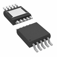
LTC1403ACMSE Linear Technology, LTC1403ACMSE Datasheet - Page 3

LTC1403ACMSE
Manufacturer Part Number
LTC1403ACMSE
Description
IC ADC 14BIT 2.8MSPS DIFF 10MSOP
Manufacturer
Linear Technology
Datasheet
1.LTC1403CMSEPBF.pdf
(20 pages)
Specifications of LTC1403ACMSE
Number Of Bits
14
Sampling Rate (per Second)
2.8M
Data Interface
Serial, SPI™
Number Of Converters
1
Power Dissipation (max)
12mW
Voltage Supply Source
Single Supply
Operating Temperature
0°C ~ 70°C
Mounting Type
Surface Mount
Package / Case
10-TFSOP, 10-MSOP (0.118", 3.00mm Width) Exposed Pad
Lead Free Status / RoHS Status
Contains lead / RoHS non-compliant
Available stocks
Company
Part Number
Manufacturer
Quantity
Price
Company:
Part Number:
LTC1403ACMSE
Manufacturer:
LT
Quantity:
10 000
Part Number:
LTC1403ACMSE#PBF
Manufacturer:
LINEAR/凌特
Quantity:
20 000
Company:
Part Number:
LTC1403ACMSE#TRPBF
Manufacturer:
SONY
Quantity:
101
Part Number:
LTC1403ACMSE#TRPBF
Manufacturer:
LINEAR/凌特
Quantity:
20 000
Company:
Part Number:
LTC1403ACMSE-1
Manufacturer:
LT
Quantity:
10 000
Company:
Part Number:
LTC1403ACMSE-1#TRPBF
Manufacturer:
LT
Quantity:
2 300
DYNAMIC ACCURACY
INTERNAL REFERENCE CHHARACTERISTICS
DIGITAL INPUTS AND DIGITAL OUTPUTS
otherwise specifi cations are at T
SYMBOL
SINAD
THD
SFDR
IMD
full operating temperature range, otherwise specifi cations are at T
PARAMETER
V
V
V
V
V
operating temperature range, otherwise specifi cations are at T
SYMBOL
V
V
I
C
V
V
I
C
I
I
IN
OZ
SOURCE
SINK
REF
REF
REF
REF
REF
IH
IL
IN
OH
OL
OZ
Output Voltage
Output Tempco
Line Regulation
Output Resistance
Settling Time
PARAMETER
Signal-to-Noise Plus
Distortion Ratio
Total Harmonic
Distortion
Spurious Free
Dynamic Range
Intermodulation
Distortion
Code-to-Code
Transition Noise
Full Power Bandwidth
Full Linear Bandwidth
PARAMETER
High Level Input Voltage
Low Level Input Voltage
Digital Input Current
Digital Input Capacitance
High Level Output Voltage
Low Level Output Voltage
Hi-Z Output Leakage D
Hi-Z Output Capacitance D
Output Short-Circuit Source Current
Output Short-Circuit Sink Current
OUT
A
= 25°C. V
OUT
CONDITIONS
100kHz Input Signal
1.4MHz Input Signal
1.4MHz Input Signal (H Grade)
100kHz Input Signal, External V
V
750kHz Input Signal, External V
V
100kHz First 5 Harmonics
1.4MHz First 5 Harmonics
100kHz Input Signal
1.4MHz Input Signal
1.25V to 2.5V 1.25MHz into A
1.2MHz into A
V
V
S/(N + D) ≥ 68dB
DD
DD
REF
IN
= 2.5V
≥ 3.3V
≥ 3.3V
= 2.5V (Note 18)
The
DD
CONDITIONS
I
V
Load Current = 0.5mA
P-P
●
OUT
= 3V
DD
denotes the specifi cations which apply over the full operating temperature range,
, SDO = 11585LSB
IN
= 2.7V to 3.6V, V
= 0
–
CONDITIONS
V
V
V
V
V
V
V
V
V
DD
DD
IN
DD
DD
DD
OUT
OUT
OUT
= 0V to V
= 3.3V
= 2.7V
= 3V, I
= 2.7V, I
= 2.7V, I
= 0V to V
= 0V, V
= V
DD
OUT
= 3V
IN
DD
OUT
OUT
A
DD
REF
REF
+
REF
P-P
= 25°C. V
DD
= –200μA
, 0V to 1.25V,
= 3V
= 160μA
= 1.6mA
A
(Note 15)
= 2.5V
= 3.3V,
= 3.3V,
= 25°C. V
DD
= 3V
The
DD
●
●
●
The
= 3V
●
MIN
●
denotes the specifi cations which apply over the full
68
67
LTC1403/LTC1403H
denotes the specifi cations which apply over the
LTC1403/LTC1403A
70.5
70.5
70.5
0.25
TYP
–87
–83
–87
–83
–82
72
72
50
5
●
●
●
●
●
●
MAX
–76
MIN
MIN
2.4
2.5
LTC1403A/LTC1403AH
MIN
70
69
TYP
0.05
0.10
600
TYP
2.5
0.2
15
2.9
20
15
2
5
1
73.5
73.5
73.0
76.3
76.3
TYP
–90
–86
–90
–86
–82
50
1
5
MAX
MAX
±10
±10
0.6
0.4
MAX
–78
ppm//°C
LSB
UNITS
UNITS
UNITS
1403fb
μV/V
3
MHz
MHz
RMS
ms
mA
mA
dB
dB
dB
dB
dB
dB
dB
dB
dB
dB
μA
μA
pF
pF
Ω
V
V
V
V
V
V


