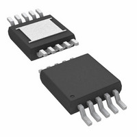
LTC1403ACMSE Linear Technology, LTC1403ACMSE Datasheet - Page 2

LTC1403ACMSE
Manufacturer Part Number
LTC1403ACMSE
Description
IC ADC 14BIT 2.8MSPS DIFF 10MSOP
Manufacturer
Linear Technology
Datasheet
1.LTC1403CMSEPBF.pdf
(20 pages)
Specifications of LTC1403ACMSE
Number Of Bits
14
Sampling Rate (per Second)
2.8M
Data Interface
Serial, SPI™
Number Of Converters
1
Power Dissipation (max)
12mW
Voltage Supply Source
Single Supply
Operating Temperature
0°C ~ 70°C
Mounting Type
Surface Mount
Package / Case
10-TFSOP, 10-MSOP (0.118", 3.00mm Width) Exposed Pad
Lead Free Status / RoHS Status
Contains lead / RoHS non-compliant
Available stocks
Company
Part Number
Manufacturer
Quantity
Price
Company:
Part Number:
LTC1403ACMSE
Manufacturer:
LT
Quantity:
10 000
Part Number:
LTC1403ACMSE#PBF
Manufacturer:
LINEAR/凌特
Quantity:
20 000
Company:
Part Number:
LTC1403ACMSE#TRPBF
Manufacturer:
SONY
Quantity:
101
Part Number:
LTC1403ACMSE#TRPBF
Manufacturer:
LINEAR/凌特
Quantity:
20 000
Company:
Part Number:
LTC1403ACMSE-1
Manufacturer:
LT
Quantity:
10 000
Company:
Part Number:
LTC1403ACMSE-1#TRPBF
Manufacturer:
LT
Quantity:
2 300
ABSOLUTE MAXIMUM RATINGS
CONVERTER CHARACTERISTICS
ANALOG INPUT
LTC1403/LTC1403A
(Note 1, 2,)
Supply Voltage (V
Analog Input Voltage
Digital Input Voltage ......................–0.3V to (V
Digital Output Voltage ...................–0.3V to (V
Power Dissipation .............................................. 100mW
Operation Temperature Range
Storage Temperature Range ................... –65°C to 150°C
Lead Temperature (Soldering, 10 sec) .................. 300°C
temperature range, otherwise specifi cations are at T
PARAMETER
Resolution (No Missing Codes)
Integral Linearity Error
Offset Error
Gain Error
Gain Tempco
specifi cations are at T
SYMBOL
V
V
I
C
t
t
t
CMRR
2
IN
ACQ
AP
JITTER
IN
CM
IN
(Note 3) ....................................–0.3V to (V
LTC1403C/LTC1403AC ............................. 0°C to 70°C
LTC1403I/LTC1403AI ........................... –40°C to 85°C
LTC1403H/LTC1403AH ...................... –40°C to 125°C
PARAMETER
Analog Differential Input Range (Notes 3, 9)
Analog Common Mode + Differential Input Range (Note 10)
Analog Input Leakage Current
Analog Input Capacitance
Sample-and-Hold Acquisition Time
Sample-and-Hold Aperture Delay Time
Sample-and-Hold Aperture Delay Time Jitter
Analog Input Common Mode Rejection Ratio
DD
A
) ..................................................4V
= 25°C. V
CONDITIONS
(Notes 4, 5, 18)
(Notes 4, 18)
(Note 4, 18)
Internal Reference (Note 4)
External Reference
The
DD
●
= 3V
denotes the specifi cations which apply over the full operating temperature range, otherwise
A
DD
DD
DD
= 25°C. With internal reference. V
●
●
●
●
+ 0.3V)
+ 0.3V)
+ 0.3V)
MIN TYP MAX MIN TYP MAX MIN TYP MAX MIN TYP MAX
–10
–30
12
–2 ±0.25
The
LTC1403
●
±15
±1
±5
±1
denotes the specifi cations which apply over the full operating
CONDITIONS
2.7V ≤ V
(Note 6)
f
f
PACKAGE/ORDER INFORMATION
IN
IN
Order Options Tape and Reel: Add #TR
Lead Free: Add #PBF Lead Free Tape and Reel: Add #TRPBF
Lead Free Part Marking:
Consult LTC Marketing for parts specifi ed with wider operating temperature ranges.
10
30
2
= 1MHz, V
= 100MHz, V
ORDER PART NUMBER
–20
–40
LTC1403CMSE
LTC1403IMSE
LTC1403HMSE
LTC1403ACMSE
LTC1403AIMSE
LTC1403AHMSE
12
–2 ±0.25
DD
LTC1403H
≤ 3.3V
IN
±15
±2
±5
±1
= 0V to 3V
IN
= 0V to 3V
20
40
V
GND
GND
DD
A
A
2
REF
IN
IN
+
–
= 3V
EXPOSED PAD IS GND (PIN 11)
http://www.linear.com/leadfree/
10-LEAD PLASTIC MSOP
MUST BE SOLDERED TO PCB
T
1
2
3
4
5
JMAX
–20
–60
14
–4
MSE PACKAGE
LTC1403A
●
●
●
= 150°C, θ
TOP VIEW
±0.5
±10
±15
±2
±1
11
MIN
JA
20
60
= 40°C/W
MSE PART MARKING
4
10
9
8
7
6
0 to V
0 to 2.5
–30
–80
14
–4
TYP
–60
–15
CONV
SCK
SDO
V
GND
0.3
13
1
DD
LTC1403AH
LTBDN
LTBDP
LTBDP
LTADF
LTAFD
LTAFD
DD
±0.5
±10
±15
±2
±1
MAX
39
1
30
80
4
ppm/°C
ppm/°C
UNITS
UNITS
1403fb
LSB
LSB
LSB
Bits
μA
dB
dB
pF
ns
ns
ps
V
V


