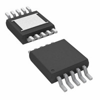
LTC1403ACMSE Linear Technology, LTC1403ACMSE Datasheet - Page 4

LTC1403ACMSE
Manufacturer Part Number
LTC1403ACMSE
Description
IC ADC 14BIT 2.8MSPS DIFF 10MSOP
Manufacturer
Linear Technology
Datasheet
1.LTC1403CMSEPBF.pdf
(20 pages)
Specifications of LTC1403ACMSE
Number Of Bits
14
Sampling Rate (per Second)
2.8M
Data Interface
Serial, SPI™
Number Of Converters
1
Power Dissipation (max)
12mW
Voltage Supply Source
Single Supply
Operating Temperature
0°C ~ 70°C
Mounting Type
Surface Mount
Package / Case
10-TFSOP, 10-MSOP (0.118", 3.00mm Width) Exposed Pad
Lead Free Status / RoHS Status
Contains lead / RoHS non-compliant
Available stocks
Company
Part Number
Manufacturer
Quantity
Price
Company:
Part Number:
LTC1403ACMSE
Manufacturer:
LT
Quantity:
10 000
Part Number:
LTC1403ACMSE#PBF
Manufacturer:
LINEAR/凌特
Quantity:
20 000
Company:
Part Number:
LTC1403ACMSE#TRPBF
Manufacturer:
SONY
Quantity:
101
Part Number:
LTC1403ACMSE#TRPBF
Manufacturer:
LINEAR/凌特
Quantity:
20 000
Company:
Part Number:
LTC1403ACMSE-1
Manufacturer:
LT
Quantity:
10 000
Company:
Part Number:
LTC1403ACMSE-1#TRPBF
Manufacturer:
LT
Quantity:
2 300
POWER REQUIREMENTS
TIMING CHARACTERISTICS
LTC1403/LTC1403A
SYMBOL
f
t
t
t
t
t
t
t
t
t
t
t
t
t
t
Note 1: Stresses beyond those listed under Absolute Maximum Ratings
may cause permanent damage to the device. Exposure to any Absolute
Maximum Rating condition for extended periods may affect device reliability
and lifetime.
Note 2: All voltage values are with respect to GND.
Note 3: When these pins are taken below GND or above V
clamped by internal diodes. This product can handle input currents greater
than 100mA below GND or greater than V
Note 4: Offset and full-scale specifi cations are measured for a single-ended
A
Note 5: Integral linearity is tested with an external 2.55V reference and is
defi ned as the deviation of a code from the straight line passing through the
actual endpoints of a transfer curve. The deviation is measured from the
center of quantization band.
Note 6: Guaranteed by design, not subject to test.
Note 7: Recommended operating conditions.
Note 8: The analog input range is defi ned for the voltage difference between
A
Note 9: The absolute voltage at A
range, otherwise specifi cations are at T
SYMBOL
V
I
P
range, otherwise specifi cations are at T
4
DD
SAMPLE(MAX)
THROUGHPUT
SCK
CONV
1
1
3
4
5
6
7
8
9
10
12
DD
D
IN
IN
+
+
input with A
and A
IN
–
PARAMETER
Supply Voltage
Positive Supply Voltage
Power Dissipation
.
PARAMETER
Maximum Sampling Frequency per Channel (Conversion Rate)
Minimum Sampling Period (Conversion + Acquisiton Period)
Clock Period
Conversion Time
Minimum Positive or Negative SCLK Pulse Width
CONV to SCK Setup Time
Nearest SCK Edge Before CONV
Minimum Positive or Negative CONV Pulse Width
SCK to Sample Mode
CONV to Hold Mode
16th SCK↑ to CONV↑ Interval (Affects Acquisition Period)
Minimum Delay from SCK to Valid Bits 0 Through 13
SCK to Hi-Z at SDO
Previous SDO Bit Remains Valid After SCK
V
REF
IN
–
grounded and using the internal 2.5V reference.
Settling Time After Sleep-to-Wake Transition
IN
+
and A
DD
IN
–
without latchup.
A
A
must be within this range.
= 25°C. (Note 17)
= 25°C. V
The
DD
The
DD
CONDITIONS
Active Mode
Active Mode (LTC1403H, LTC1403AH)
Nap Mode
Nap Mode (LTC1403H, LTC1403AH)
Sleep Mode (LTC1403, LTC1403H)
Sleep Mode (LTC1403A, LTC1403AH)
Active Mode with SCK in Fixed State (Hi or Lo)
, they will be
●
= 3V
denotes the specifi cations which apply over the full operating temperature
●
denotes the specifi cations which apply over the full operating temperature
Note 10: If less than 3ns is allowed, the output data will appear one clock
cycle later. It is best for CONV to rise half a clock before SCK, when running
the clock at rated speed.
Note 11: Not the same as aperture delay. Aperture delay is smaller (1ns)
because the 2.2ns delay through the sample-and-hold is subtracted from
the CONV to Hold mode delay.
Note 12: The rising edge of SCK is guaranteed to catch the data coming out
into a storage latch.
Note 13: The time period for acquiring the input signal is started by the
16th rising clock and it is ended by the rising edge of convert.
Note 14: The internal reference settles in 2ms after it wakes up from Sleep
mode with one or more cycles at SCK and a 10μF capacitive load.
Note 15: The full power bandwidth is the frequency where the output code
swing drops to 3dB with a 2.5V
Note 16: Maximum clock period guarantees analog performance during
conversion. Output data can be read without an arbitrarily long clock.
Note 17: V
Note 18: The LTC1403A is measured and specifi ed with 14-bit Resolution
(1LSB = 152μV) and the LTC1403 is measured and specifi ed with 12-bit
Resolution (1LSB = 610μV).
CONDITIONS
(Notes 16)
(Note 6)
(Note 6)
(Notes 6, 10)
(Note 6)
(Note 6)
(Note 6)
(Notes 6, 11)
(Notes 6, 7, 13)
(Notes 6, 12)
(Notes 6, 12)
(Notes 6, 12)
(Notes 6, 14)
DD
= 3V, f
SAMPLE
●
●
●
●
= 2.8Msps.
●
●
●
P-P
MIN
19.8
2.8
1.2
MIN
16
45
input sine wave.
2.7
2
3
0
4
4
8
6
2
TYP
18
2
TYP
4.7
5.2
1.1
1.2
12
2
2
10000
MAX
357
MAX
3.6
1.5
1.8
15
10
7
8
SCLK cycles
UNITS
UNITS
1403fb
MHz
mW
mA
mA
mA
mA
ms
μA
μA
ns
ns
ns
ns
ns
ns
ns
ns
ns
ns
ns
ns
V


