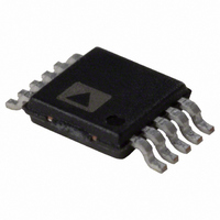
AD5173BRM2.5-RL7 Analog Devices Inc, AD5173BRM2.5-RL7 Datasheet - Page 14

AD5173BRM2.5-RL7
Manufacturer Part Number
AD5173BRM2.5-RL7
Description
IC DGTL POT DUAL 2.5K OTP 10MSOP
Manufacturer
Analog Devices Inc
Datasheet
1.AD5172BRMZ2.5.pdf
(24 pages)
Specifications of AD5173BRM2.5-RL7
Rohs Status
RoHS non-compliant
Taps
256
Resistance (ohms)
2.5K
Number Of Circuits
2
Temperature Coefficient
35 ppm/°C Typical
Memory Type
Non-Volatile
Interface
I²C, 2-Wire Serial
Voltage - Supply
2.7 V ~ 5.5 V
Operating Temperature
-40°C ~ 125°C
Mounting Type
Surface Mount
Package / Case
10-MSOP, Micro10™, 10-uMAX, 10-uSOP
Resistance In Ohms
2.5K
Number Of Elements
2
# Of Taps
256
Resistance (max)
2.5KOhm
Power Supply Requirement
Single
Interface Type
Serial (2-Wire/I2C)
Single Supply Voltage (typ)
3/5V
Dual Supply Voltage (typ)
Not RequiredV
Single Supply Voltage (min)
2.7V
Single Supply Voltage (max)
5.5V
Dual Supply Voltage (min)
Not RequiredV
Dual Supply Voltage (max)
Not RequiredV
Operating Temp Range
-40C to 125C
Operating Temperature Classification
Automotive
Mounting
Surface Mount
Pin Count
10
Lead Free Status / RoHS Status
Not Compliant
AD5172/AD5173
TEST CIRCUITS
Figure 31 to Figure 38 illustrate the test circuits that define the test conditions used in the product specification tables (see Table 1 and Table 2).
Figure 32. Resistor Position Nonlinearity Error (Rheostat Operation: R-INL, R-DNL)
Figure 31. Potentiometer Divider Nonlinearity Error (INL, DNL)
V
V+
MS2
Figure 34. Power Supply Sensitivity (PSS, PSSR)
V
DD
V+
V
NC = NO CONNECT
A
NC
A
B
A
DUT
B
DUT
A
B
DUT
Figure 33. Wiper Resistance
W
W
A
DUT
B
W
W
V
W
V
MS1
V
MS
PSRR (dB) = 20 log
PSS (%/%) =
V+ = V
I
W
V
1LSB = V+/2
V+ = V
MS
= V
V
R
MS
DD
DD
W
I
W
= [V
DD
/R
± 10%
NOMINAL
MS1
Δ
ΔV
N
V
MS
DD
– V
%
%
MS2
(
ΔV
ΔV
]/I
MS
DD
W
)
Rev. H | Page 14 of 24
OFFSET
GND
V
Figure 35. Test Circuit for Gain vs. Frequency
Figure 37. Common-Mode Leakage Current
IN
V
IN
Figure 36. Incremental On Resistance
NC = NO CONNECT
2.5V
DUT
V
B
DD
Figure 38. Analog Crosstalk
NC
CTA = 20 log[V
NC = NO CONNECT
DUT
GND
W1
RDAC1
A1
W
I
SW
GND TO V
A
B
NC
NC
B1
DUT
A
B
R
CODE = 0x00
SW
W
W
V
V
=
DD
SS
DD
0.1V
OUT
I
SW
I
V
CM
AD8610
CM
RDAC2
/V
+5V
–5V
IN
W2
A2
B2
0.1V
]
V
OUT
V
OUT


