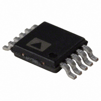
AD5173BRM2.5-RL7 Analog Devices Inc, AD5173BRM2.5-RL7 Datasheet - Page 15

AD5173BRM2.5-RL7
Manufacturer Part Number
AD5173BRM2.5-RL7
Description
IC DGTL POT DUAL 2.5K OTP 10MSOP
Manufacturer
Analog Devices Inc
Datasheet
1.AD5172BRMZ2.5.pdf
(24 pages)
Specifications of AD5173BRM2.5-RL7
Rohs Status
RoHS non-compliant
Taps
256
Resistance (ohms)
2.5K
Number Of Circuits
2
Temperature Coefficient
35 ppm/°C Typical
Memory Type
Non-Volatile
Interface
I²C, 2-Wire Serial
Voltage - Supply
2.7 V ~ 5.5 V
Operating Temperature
-40°C ~ 125°C
Mounting Type
Surface Mount
Package / Case
10-MSOP, Micro10™, 10-uMAX, 10-uSOP
Resistance In Ohms
2.5K
Number Of Elements
2
# Of Taps
256
Resistance (max)
2.5KOhm
Power Supply Requirement
Single
Interface Type
Serial (2-Wire/I2C)
Single Supply Voltage (typ)
3/5V
Dual Supply Voltage (typ)
Not RequiredV
Single Supply Voltage (min)
2.7V
Single Supply Voltage (max)
5.5V
Dual Supply Voltage (min)
Not RequiredV
Dual Supply Voltage (max)
Not RequiredV
Operating Temp Range
-40C to 125C
Operating Temperature Classification
Automotive
Mounting
Surface Mount
Pin Count
10
Lead Free Status / RoHS Status
Not Compliant
THEORY OF OPERATION
The AD5172/AD5173 are 256-position, digitally controlled
variable resistors (VRs) that employ fuse link technology to
achieve memory retention of the resistance setting.
An internal power-on preset places the wiper at midscale
during power-on. If the OTP function is activated, the device
powers up at the user-defined permanent setting.
ONE-TIME PROGRAMMING (OTP)
Prior to OTP activation, the AD5172/AD5173 presets to midscale
during initial power-on. After the wiper is set to the desired
position, the resistance can be permanently set by programming
the T bit high, with the proper coding (see Table 8 and Table 9),
and one-time V
family of digital potentiometers requires V
5.6 V and 5.8 V to blow the fuses to achieve a given nonvolatile
setting. However, during operation, V
result, an external supply is required for one-time programming.
The user is allowed only one attempt to blow the fuses. If the user
fails to blow the fuses during this attempt, the structure of the
fuses can change such that they may never be blown, regardless
of the energy applied during subsequent events. For details, see
the Power Supply Considerations section.
The device control circuit has two validation bits, E1 and E0,
that can be read back to check the programming status (see
Table 7). Users should always read back the validation bits to
ensure that the fuses are properly blown. After the fuses are
blown, all fuse latches are enabled upon subsequent power-on;
therefore, the output corresponds to the stored setting. Figure 39
shows a detailed functional block diagram.
DD_OTP
. The fuse link technology of the AD517x
SDA
SCL
DD
can be 2.7 V to 5.5 V. As a
CONTROL BLOCK
PROGRAM/TEST
I
DD_OTP
2
C INTERFACE
ONE-TIME
COMPARATOR
to be between
Figure 39. Detailed Functional Block Diagram
Rev. H | Page 15 of 24
FUSES
DAC
REG
EN
Table 7. Validation Status
E1
0
1
1
PROGRAMMING THE VARIABLE RESISTOR AND
VOLTAGE
Rheostat Operation
The nominal resistance of the RDAC between Terminal A and
Terminal B is available in 2.5 kΩ, 10 kΩ, 50 kΩ, and 100 kΩ.
The nominal resistance (R
accessed by the wiper terminal and the B terminal contact. The
8-bit data in the RDAC latch is decoded to select one of the
256 possible settings.
Assuming a 10 kΩ part is used, the first connection of the wiper
starts at the B terminal for Data 0x00. Because there is a 50 Ω
wiper contact resistance, such a connection yields a minimum
of 100 Ω (2 × 50 Ω) resistance between Terminal W and Ter-
minal B. The second connection is the first tap point, which
corresponds to 139 Ω (R
50 Ω) for Data 0x01. The third connection is the next tap point,
representing 178 Ω (2 × 39 Ω + 2 × 50 Ω) for Data 0x02, and so
on. Each LSB data value increase moves the wiper up the resistor
ladder until the last tap point is reached at 10,100 Ω (R
MUX
E0
0
0
1
FUSE
REG
A
B
Status
Ready for programming.
Fatal error. Some fuses are not blown. Do not retry.
Discard this unit.
Successful. No further programming is possible.
DECODER
W
Figure 40. Rheostat Mode Configuration
WB
A
B
AB
= R
) of the VR has 256 contact points
AB
W
/256 + 2 × R
A
W
B
AD5172/AD5173
A
B
W
= 39 Ω + 2 ×
W
AB
+ 2 × R
W
).


