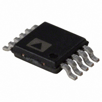
AD5173BRM2.5-RL7 Analog Devices Inc, AD5173BRM2.5-RL7 Datasheet - Page 8

AD5173BRM2.5-RL7
Manufacturer Part Number
AD5173BRM2.5-RL7
Description
IC DGTL POT DUAL 2.5K OTP 10MSOP
Manufacturer
Analog Devices Inc
Datasheet
1.AD5172BRMZ2.5.pdf
(24 pages)
Specifications of AD5173BRM2.5-RL7
Rohs Status
RoHS non-compliant
Taps
256
Resistance (ohms)
2.5K
Number Of Circuits
2
Temperature Coefficient
35 ppm/°C Typical
Memory Type
Non-Volatile
Interface
I²C, 2-Wire Serial
Voltage - Supply
2.7 V ~ 5.5 V
Operating Temperature
-40°C ~ 125°C
Mounting Type
Surface Mount
Package / Case
10-MSOP, Micro10™, 10-uMAX, 10-uSOP
Resistance In Ohms
2.5K
Number Of Elements
2
# Of Taps
256
Resistance (max)
2.5KOhm
Power Supply Requirement
Single
Interface Type
Serial (2-Wire/I2C)
Single Supply Voltage (typ)
3/5V
Dual Supply Voltage (typ)
Not RequiredV
Single Supply Voltage (min)
2.7V
Single Supply Voltage (max)
5.5V
Dual Supply Voltage (min)
Not RequiredV
Dual Supply Voltage (max)
Not RequiredV
Operating Temp Range
-40C to 125C
Operating Temperature Classification
Automotive
Mounting
Surface Mount
Pin Count
10
Lead Free Status / RoHS Status
Not Compliant
AD5172/AD5173
PIN CONFIGURATIONS AND FUNCTION DESCRIPTIONS
Table 5. AD5172 Pin Function Descriptions
Pin
No.
1
2
3
4
5
6
7
8
9
10
Mnemonic
B1
A1
W2
GND
V
SCL
SDA
A2
B2
W1
DD
Figure 4. AD5172 Pin Configuration
GND
V
W2
B1
A1
DD
Description
B1 Terminal. GND ≤ V
A1 Terminal. GND ≤ V
W2 Terminal. GND ≤ V
Digital Ground.
Positive Power Supply. Specified for
operation from 2.7 V to 5.5 V. For OTP
programming, V
of 5.6 V but no more than 5.8 V and to be
capable of driving 100 mA.
Serial Clock Input. Positive-edge triggered.
Requires a pull-up resistor. If this pin is driven
directly from a logic controller without a
pull-up resistor, ensure that the V
is 0.7 V × V
Serial Data Input/Output. Requires a pull-up
resistor. If this pin is driven directly from a
logic controller without a pull-up resistor,
ensure that the V
A2 Terminal. GND ≤ V
B2 Terminal. GND ≤ V
W1 Terminal. GND ≤ V
1
2
3
4
5
(Not to Scale)
AD5172
TOP VIEW
DD
.
DD
IH
10
9
8
7
6
needs to be a minimum
minimum is 0.7 V × V
W1
B2
A2
SDA
SCL
B1
B2
A1
A2
W2
W1
≤ V
≤ V
≤ V
≤ V
≤ V
≤ V
DD
DD
DD
DD
DD
DD
.
.
.
.
.
.
IH
minimum
DD
Rev. H | Page 8 of 24
.
Table 6. AD5173 Pin Function Descriptions
Pin
No.
1
2
3
4
5
6
7
8
9
10
Mnemonic
B1
AD0
W2
GND
V
SCL
SDA
AD1
B2
W1
DD
Figure 5. AD5173 Pin Configuration
GND
AD0
V
W2
B1
DD
Description
B1 Terminal. GND ≤ V
Programmable Address Bit 0 for Multiple
Package Decoding.
W2 Terminal. GND ≤ V
Digital Ground.
Positive Power Supply. Specified for
operation from 2.7 V to 5.5 V. For OTP
programming, V
of 5.6 V but no more than 5.8 V and to be
capable of driving 100 mA.
Serial Clock Input. Positive-edge triggered.
Requires a pull-up resistor. If this pin is driven
directly from a logic controller without a
pull-up resistor, ensure that the V
is 0.7 V × V
Serial Data Input/Output. Requires a pull-up
resistor. If this pin is driven directly from a
logic controller without a pull-up resistor,
ensure that the V
Programmable Address Bit 1 for Multiple
Package Decoding.
B2 Terminal. GND ≤ V
W1 Terminal. GND ≤ V
1
2
3
4
5
(Not to Scale)
AD5173
TOP VIEW
DD
.
DD
IH
10
9
8
7
6
needs to be a minimum
minimum is 0.7 V × V
W1
B2
AD1
SDA
SCL
B1
B2
W2
W1
≤ V
≤ V
≤ V
≤ V
DD
DD
DD
DD
.
.
.
.
IH
minimum
DD
.


