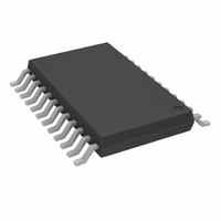
AD8403ARU100-REEL Analog Devices Inc, AD8403ARU100-REEL Datasheet - Page 21

AD8403ARU100-REEL
Manufacturer Part Number
AD8403ARU100-REEL
Description
IC POT DIG QUAD 100K 8B 24TSSOP
Manufacturer
Analog Devices Inc
Datasheet
1.AD8400ARZ1.pdf
(32 pages)
Specifications of AD8403ARU100-REEL
Rohs Status
RoHS non-compliant
Taps
256
Resistance (ohms)
100K
Number Of Circuits
4
Temperature Coefficient
500 ppm/°C Typical
Memory Type
Volatile
Interface
SPI, 3-Wire Serial
Voltage - Supply
2.7 V ~ 5.5 V
Operating Temperature
-40°C ~ 125°C
Mounting Type
Surface Mount
Package / Case
24-TSSOP
Resistance In Ohms
100K
Number Of Elements
4
# Of Taps
256
Resistance (max)
100KOhm
Power Supply Requirement
Single
Interface Type
Serial (3-Wire/SPI)
Single Supply Voltage (typ)
3/5V
Dual Supply Voltage (typ)
Not RequiredV
Single Supply Voltage (min)
2.7V
Single Supply Voltage (max)
5.5V
Dual Supply Voltage (min)
Not RequiredV
Dual Supply Voltage (max)
Not RequiredV
Operating Temp Range
-40C to 125C
Operating Temperature Classification
Automotive
Mounting
Surface Mount
Pin Count
24
Package Type
TSSOP
For Use With
AD8403EVAL - BOARD EVAL FOR AD8403
Lead Free Status / Rohs Status
Not Compliant
Available stocks
Company
Part Number
Manufacturer
Quantity
Price
Company:
Part Number:
AD8403ARU100-REEL
Manufacturer:
A/D
Quantity:
280
Part Number:
AD8403ARU100-REEL
Manufacturer:
ADI/亚德诺
Quantity:
20 000
Like a mechanical potentiometer, RDAC is symmetrical. The
resistance between the Wiper W and Terminal A also produces
a digitally controlled complementary resistance, R
these terminals are used, the B terminal can be tied to the wiper
or left floating. R
data loaded into the RDAC latch increases. The general transfer
equation for this R
where D is the data loaded into the 8-bit RDAC# latch, and R
is the nominal end-to-end resistance.
For example, when the B terminal is either open-circuited or
tied to the Wiper W, the following RDAC latch codes result in
the following R
Table 11.
D (Dec)
255
128
1
0
The typical distribution of RAB from channel to channel
matches within ±1%. However, device-to-device matching
is process lot dependent and has a ±20% variation. The tem-
perature coefficient, or the change in R
is 500 ppm/°C.
The wiper-to-end-terminal resistance temperature coefficient
has the best performance over the 10% to 100% of adjustment
range where the internal wiper contact switches do not con-
tribute any significant temperature related errors. The graph in
Figure 18 shows the performance of R
the potentiometer with codes below 32 results in the larger
temperature coefficients plotted.
PROGRAMMING THE POTENTIOMETER DIVIDER
Voltage Output Operation
The digital potentiometer easily generates an output voltage
proportional to the input voltage applied to a given terminal.
For example, connecting the A terminal to 5 V and the B termi-
nal to ground produces an output voltage at the wiper starting
at 0 V up to 1 LSB less than 5 V. Each LSB is equal to the voltage
applied across the A to B terminals divided by the 256-position
resolution of the potentiometer divider. The general equation
defining the output voltage with respect to ground for any given
input voltage applied to the A to B terminals is
Operation of the digital potentiometer in the voltage divider
mode results in more accurate operation over temperature.
V
R
W
WA
=
( )
R
89
5,050
10,011
10,050
D
WA
WA
256
D
WA
=
(Ω)
(for the 10 kΩ version):
WA
256
×
starts at the maximum and decreases as the
V
is
256
AB
−
+
D
V
Output State
Full-Scale
Midscale ( RS = 0 Condition)
1 LSB
Zero-Scale
×
B
R
AB
+
R
W
WB
AB
tempco vs. code. Using
with temperature,
WA
. When
Rev. E | Page 21 of 32
AB
(3)
(4)
Here the output voltage is dependent on the ratio of the internal
resistors, not the absolute value; therefore, the temperature drift
improves to 15 ppm/°C.
At the lower wiper position settings, the potentiometer divider
temperature coefficient increases because the contribution of
the CMOS switch wiper resistance becomes an appreciable
portion of the total resistance from the B terminal to the
Wiper W. See Figure 17 for a plot of potentiometer tempco
performance vs. code setting.
DIGITAL INTERFACING
The AD8400/AD8402/AD8403 contain a standard SPI-
compatible, 3-wire, serial input control interface. The three
inputs are clock (CLK), chip select ( CS ), and serial data input
(SDI). The positive-edge sensitive CLK input requires clean
transitions to avoid clocking incorrect data into the serial input
register. For the best result, use logic transitions faster than
1 V/μs. Standard logic families work well. If mechanical switches
are used for product evaluation, they should be debounced by
a flip-flop or other suitable means. The block diagrams in
Figure 46 Figure 47
circuitry in more detail. When
loads data into the 10-bit serial register on each positive clock
edge (see
SHDN
CLK
CLK
SDI
SDI
CS
CS
,
Table 12
DGND
DI D0
10-BIT
DI
10-BIT
SER
REG
REG
SER
A1
A0
D7
Figure 46. AD8400 Block Diagram
Figure 47. AD8402 Block Diagram
).
A1
A0
D7
D0
, and
8
8
ADDR
ADDR
DEC
DEC
EN
EN
AD8400/AD8402/AD8403
Figure 48
RS
CS is taken active low, the clock
D7
D0
D7
D0
D7
D0
LATCH
show the internal digital
RDAC
LATCH
LATCH
NO. 1
RDAC
RDAC
NO. 1
NO. 2
AD8400
R
R
AD8402
AGND
GND
V
A1
W1
B1
V DD
A1
W1
B1
A4
W4
B4
DD


