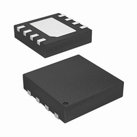
ISL95810UIRT8Z Intersil, ISL95810UIRT8Z Datasheet - Page 10

ISL95810UIRT8Z
Manufacturer Part Number
ISL95810UIRT8Z
Description
IC XDCP 256-TAP 50KOHM 8-TDFN
Manufacturer
Intersil
Series
XDCP™r
Datasheet
1.ISL95810WIU8Z.pdf
(13 pages)
Specifications of ISL95810UIRT8Z
Taps
256
Resistance (ohms)
50K
Number Of Circuits
1
Temperature Coefficient
45 ppm/°C Typical
Memory Type
Non-Volatile
Interface
I²C, 2-Wire Serial
Voltage - Supply
2.7 V ~ 5.5 V
Operating Temperature
-40°C ~ 85°C
Mounting Type
Surface Mount
Package / Case
8-TDFN
Resistance In Ohms
50K
Lead Free Status / RoHS Status
Lead free / RoHS Compliant
Write Operation
A Write operation requires a START condition, followed by a
valid Identification Byte, a valid Address Byte, a Data Byte,
and a STOP condition. After each of the three bytes, the
ISL95810 responds with an ACK. At this time, if the Data
Byte is to be written only to volatile registers, then the device
enters its standby state. If the Data Byte is to be written also
to non-volatile memory, the ISL95810 begins its internal
write cycle to non-volatile memory. During the internal non-
volatile write cycle, the device ignores transitions at the SDA
and SCL pins, and the SDA output is at a high impedance
state. When the internal non-volatile write cycle is
completed, the ISL95810 enters its standby state (See
Figure 17).
SIGNAL AT SDA
FROM THE
SIGNALS
MASTER
SIGNALS FROM
SDA OUTPUT FROM
SDA OUTPUT FROM
THE SLAVE
TRANSMITTER
S
T
A
R
T
SCL FROM
RECEIVER
MASTER
0
IDENTIFICATION
1
BYTE WITH
SIGNALS FROM
SIGNAL AT SDA
SIGNALS FROM
0
R/W=0
THE MASTER
THE ISL95810
1
10
0 0 0
START
0
FIGURE 16. ACKNOWLEDGE RESPONSE FROM RECEIVER
A
C
K
0 0 0
HIGH IMPEDANCE
ADDRESS
S
A
R
T
T
BYTE
0
FIGURE 17. BYTE WRITE SEQUENCE
0
IDENTIFICATION
0 0
1
1
FIGURE 18. READ SEQUENCE
0
BYTE
1
0
A
C
K
0
ISL95810
S
A
R
0
T
T
WRITE
0
0
IDENTIFICATION
A
C
K
1
BYTE WITH
0
0 0 0 0
R/W=1
1
ADDRESS
The byte at address 02h determines if the Data Byte is to be
written to volatile and/or non-volatile memory (See “Memory
Description” on page 8).
Data Protection
The WP pin has to be at logic HIGH to perform any Write
operation to the device. When the WP is active (LOW) the
device ignores Data Bytes of a Write Operation, does not
respond to the Data Bytes with an ACK, and instead, goes to
its standby state waiting for a new START condition.
A STOP condition also acts as a protection of non-volatile
memory. A valid Identification Byte, Address Byte, and total
number of SCL pulses act as a protection of both volatile
and non-volatile registers. During a Write sequence, the
Data Byte is loaded into an internal shift register as it is
0 0 0
BYTE
0 0 0 0
1
A
C
K
A
C
K
8
FIRST READ
DATA BYTE
DATA
BYTE
A
C
K
HIGH IMPEDANCE
ACK
9
A
C
K
A
C
K
S
T
O
P
LAST READ
DATA BYTE
September 19, 2006
FN8090.2
O
S
T
P


